5.1 Introduction
State space averaging method [1] is a commonly used method for analyzing switching power converters. But there are obvious limitations [2–7] with the average model as it is independent on the switching frequency. In particular, it is not easy to analyze ripples, or explain the DC offset phenomenon when the switching power converter operates with quite low switching frequency [3]. And the proposed improvement of the average method or the general average method in [2–7] is too cumbersome and difficult to be understood. Equivalent small parameter method (ESPM) [8–11] combines the advantages of the perturbation method and the harmonic balance method, without the need for artificial introduction of small parameters, is a symbolic analysis method with higher precision and relatively simple analysis procedure, and is suitable for analysis of strong nonlinear high-order system. In [12–18], The ESPM is used for analysis of open-loop power converters with continuous current mode (CCM), discontinuous-current-mode (DCM), multi-topology mode operation (including multiple switch converters), as well as in the steady state analysis of Class E amplifiers. And the analytical expression of the converters output ripple can be obtained.
The basic principles of the ESPM together with its applications in the steady-state and transient solutions of open-loop PWM switching power converters are systematically illustrated in Chaps. 3 and 4 respectively. And this chapter begins to apply the equivalent small parameter method (ESP) to the analysis of closed-loop systems. In Chaps. 5 and 6, this symbol analysis method is extended to the closed-loop Voltage-Mode-Controlled (VMC) PWM switching power converter system with CCM and DCM operation. The analytic solutions of the state variable ripples and the duty cycle of the closed-loop system can be obtained. Based on these analytical solutions, the effect of ripple on the duty cycle and the relationship between the DC offset in the converter and the operating frequency can be directly explained. At the same time, the examples show that increasing the integral capacitance in the feedback control loop can properly compensate for the DC drift existing in the system. In view of the fact that the Current-Mode-Control (CMC) has more advantages than the duty cycle programmed control (i.e., voltage-mode-control), we will establish the equivalent small-parameter symbol analysis method of the closed-loop PWM converter system with current-mode-control in Chap. 7. In Chap. 8, we further extend the ESPM to the analysis of frequency-modulated (FM) quasi-resonant converters to show the applicability of the method.
In Sects. 5.2 and 5.3, we first discuss in detail the establishment of the mathematical model of the closed-loop PWM converter system, and then propose the basic algorithm of the closed-loop system based on the equivalent small parameter method. Section 5.4 gives an example analysis and comparison of ESPM and numerical simulations. Section 5.5 proposes a double iterative method to improve the basic algorithm and improve its convergence and accuracy. The experimental results for further verification of the analysis for open-loop and closed-loop converters based on the ESPM are introduced in Sect. 5.6, and the summary of this chapter is given in Sect. 5.7 finally.
5.2 Modeling the Closed-Loop VMC-PWM Converter with CCM Operation
5.2.1 Mathematical Description of the Closed-Loop System


 , in which e1 is a constant vector, and
  when
when  . According to (5.1) and (5.2), one can get the following matrix equation as
![$$\left[ {\begin{array}{*{20}c} {{\mathbf{g}}_{1} (p)} & 0 \\ {\mathbf{F}} & {{\mathbf{g}}_{3} (p)} \\ \end{array} } \right]{\kern 1pt} \left[ {\begin{array}{*{20}c} {{\mathbf{x}}_{1} } \\ {{\mathbf{x}}_{2} } \\ \end{array} } \right] + \left[ {\begin{array}{*{20}c} {{\mathbf{g}}_{2} (p)} & 0 \\ 0 & 0 \\ \end{array} } \right]\delta (t)\left( {\left[ {\begin{array}{*{20}c} {{\mathbf{e}}_{1} } \\ 0 \\ \end{array} } \right] + \left[ {\begin{array}{*{20}c} {{\mathbf{x}}_{1} } \\ {{\mathbf{x}}_{2} } \\ \end{array} } \right]} \right) = \left[ {\begin{array}{*{20}c} {{\mathbf{u}}_{1} } \\ {{\mathbf{u}}_{2} } \\ \end{array} } \right]$$](../images/419194_1_En_5_Chapter/419194_1_En_5_Chapter_TeX_Equ3.png)

 . The meaning of each item in Eq. (5.4) can be obtained by referring to Eq. (5.3), where x represents the state variables of the whole closed-loop system (including the power stage main circuit and the feedback control circuit). It can be seen that the mathematical model of the closed-loop system is exactly the same in form as that of the open-loop system. The switch function
  (hereinafter,
  is sometimes abbreviated as
  ) indicates the on (off) state of the main switch in the circuit, respectively. For CCM-operated converter, the switching function is defined as
Here T denotes the switching cycle, and d(t) (abbreviated as d) is duty cycle. In the open loop, d(t) is a constant value of D, while in the case of closed-loop, d(t) is determined by the state variable and the feedback control law.
This method is suitable for higher order converters, and Eqs. (5.1) and (5.2) can be generalized to more complex circuits. For the sake of simplicity, this chapter discusses the case where the main circuit is second order, that is, the main circuit has only one inductor L and one capacitor C, and the inductor current along with the capacitor voltage are taken as the main circuit state variable vector, i.e. x1 = [iLvc]Tr, where the superscript “Tr” indicates that the matrix is transposed.
5.2.2 Expression of the Duty Cycle d
5.2.2.1 Expression of d with Proportional Feedback Control
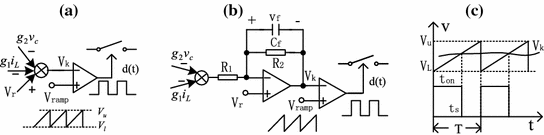
a Proportional feedback control, b proportional-integral feedback control, c diagram of duty cycle


Here the coefficient  , and the vector
 ![$${\mathbf{K}}_{1} = \left[ {\begin{array}{*{20}c} {\frac{{ - g_{1} }}{{V_{u} - V_{L} }}} & {\frac{{ - g_{2} }}{{V_{u} - V_{L} }}} \\ \end{array} } \right]$$](../images/419194_1_En_5_Chapter/419194_1_En_5_Chapter_TeX_IEq9.png) , in which Vu and VL are the maximum and minimum values of the sawtooth wave, respectively.
, in which Vu and VL are the maximum and minimum values of the sawtooth wave, respectively.
5.2.2.2 Expression of d with Proportional-Integral Feedback Control


Here the state variables of the closed-loop system with PI control is chosen as ![$${\mathbf{x}} = \left[ {\begin{array}{*{20}c} {i_{L\;} } & {v_{C\;} } & {v_{f} } \\ \end{array} } \right]\;^{{{\text{T}}r}}$$](../images/419194_1_En_5_Chapter/419194_1_En_5_Chapter_TeX_IEq10.png) , the coefficient
, the coefficient  , and the coefficient row vector is.
 ![$${\mathbf{K}}_{1} = \quad \left[ {\begin{array}{*{20}c} 0 & 0 & {\frac{ - 1}{{V_{u} - V_{L} }}} \\ \end{array} } \right]$$](../images/419194_1_En_5_Chapter/419194_1_En_5_Chapter_TeX_IEq12.png) .
.
 can be developed into a series as:
 contains the main oscillation component of
  . The mark
  is used to indicate that
  , that is
  is an i-ordered small amount of
  . When a specific value is needed for calculation, let
  . Similarly, expand the duty cycle
  into the sum of the main item and the correction quantity as follows.


 as
as
It is easy to know from (5.15) that ts0 represents the moment when the comparator is flipped with only the principal component x0 being contained into the steady-state periodic solution x. And ts1 corresponds to the moment that the comparator is flipped when x contains the main component x0 and the first-order correction term x1. Similarly, ts2 corresponds to the flip moment when x contains the terms x0, x1 and x2, and so on.


 . Considering that the general ripple has little effect on the duty cycle, which can be explained from the following example, to simplify the calculation, we use the first-order approximation of the Taylor series to find the term di. Meanwhile, according to iterative solution, when seeking to find
  , the terms
  are already known. Therefore the following equations can be obtained.


 on both sides of the equation gives:


It can be seen from the above analysis that, for the closed-loop PWM switching converter system, no matter how complex the feedback control circuit is, take the power stage main circuit and feedback control circuit as a whole during analysis, then the state equation for a closed-loop system can be written in a uniform form similar to that of an open-loop system. And the duty cycle can be expressed as a linear combination of state variables (such as (5.8) or (5.10)).
5.2.3 Series Expansion of Switching Function δ(t) for Closed-Loop Systems
 defined by (5.5) can still be expanded into a Fourier series as
![$$\delta = b_{0} + \sum\limits_{m = 1}^{\infty } {[b_{m} \exp (jm\tau ) + \bar{b}_{m} \exp ( - jm\tau )]}$$](../images/419194_1_En_5_Chapter/419194_1_En_5_Chapter_TeX_Equ24.png)
 represents the conjugate pair of the term
  , which can be found by the following equation as


![$$\begin{aligned} \delta & = \left[ {d_{0} + \sum\limits_{m = 1}^{\infty } {(b_{m0} e^{jm\tau } + c.c)} } \right] + \varepsilon \left[ {d_{1} + \sum\limits_{m = 1}^{\infty } {(b_{m1} e^{jm\tau } + c.c)} } \right] \\ & \quad + \varepsilon^{2} \left[ {d_{2} + \sum\limits_{m = 1}^{\infty } {(b_{m2} e^{jm\tau } + c.c)} } \right] + \cdots \\ \end{aligned}$$](../images/419194_1_En_5_Chapter/419194_1_En_5_Chapter_TeX_Equ34.png)


 is defined as

So far, the discrete time-varying differential equations represented by (5.4) can be transformed into a state differential equation with continuous time by the transformation of (5.31). Therefore, the equivalent small parameter can be adopted to obtain the analytic solution of the closed-loop system.
5.3 Solution of the Time-Varying Closed-Loop System with CCM Operation
The closed-loop time-varying differential equation (5.4) is solved by using equivalent small parametric method now. Since (5.4) has the same form as the open-loop state equation (5.1), the basic principle of solving is the same as the open-loop system. The difference is that the duty cycle  is not a constant, but a variable associated with the feedback circuit and the state variable (see (5.8) or (5.10)). The switching function defined by (5.5) is expanded in series shown in Eq. (5.31). For the sake of simplicity, we only consider the case of
  in Eq. (5.4).
 is expressed as the sum of the main wave x0 and the corrections xi, as shown in (5.11). Similarly the nonlinear vector function f is still expanded into the sum of the main term f0 and the correction terms fi, and they are determined by the following expressions as

5.3.1 Solution of Main Component


![$$\left[ {{\mathbf{G}}_{0} (0) + {\mathbf{G}}_{1} (0)d_{0} } \right]{\mathbf{a}}_{00} = {\mathbf{u}}$$](../images/419194_1_En_5_Chapter/419194_1_En_5_Chapter_TeX_Equ44.png)

The solutions of a00 and d0 can be obtained by combining Eqs. (5.38) and (5.37). Generally, for closed-loop systems, the solutions of a00 and d0 are non-linear and depend on the specific main circuit and feedback control law. The specific solution process can be analyzed with reference to the following examples.
5.3.2 Solution of the First-Order Correction
 in (5.36) contains the fundamental wave only, the first-order correction x1 can be assumed that
 , we can get


![$$[{\mathbf{G}}{}_{0}(j\omega ) + {\mathbf{G}}_{1} (j\omega ) \cdot d_{0} ] \cdot {\mathbf{a}}_{11} = - {\mathbf{G}}_{1} (j\omega ) \cdot (b_{11} + b_{10} ) \cdot {\mathbf{a}}_{00}$$](../images/419194_1_En_5_Chapter/419194_1_En_5_Chapter_TeX_Equ48.png)
![$$\begin{aligned} b_{10} & = [\sin 2\pi d_{0} - j(1 - \cos 2\pi d_{0} )]/2\pi \\ b_{11} & = d_{1} \cdot (\cos 2\pi d_{0} - j\sin 2\pi d_{0} ) = d_{1} \cdot e^{{ - j\tau_{s0} }} \;(\tau_{s0} = 2\pi d_{0} ) \\ \end{aligned}$$](../images/419194_1_En_5_Chapter/419194_1_En_5_Chapter_TeX_Equ49.png)

![$$\begin{aligned} d_{1} & = B_{1} /A_{1} \\ {\mathbf{a}}_{11} & = {\mathbf{G}}^{ - 1} (j\omega ) \cdot [ - {\mathbf{G}}_{1} (j\omega ) \cdot (d_{1} e^{{ - j\tau_{s0} }} + b_{10} ) \cdot {\mathbf{a}}_{00} ] \\ \end{aligned}$$](../images/419194_1_En_5_Chapter/419194_1_En_5_Chapter_TeX_Equ51.png)


As can be seen from (5.42), in the approximate calculation, the first order correction can be obtained by solving the linear equations.
5.3.3 Solution of the Second-Order Correction
 in (5.40), one can assume the second-order correction term x2 can be expressed as
 and
and  into
into  , one can get
  as
as
 of the second harmonic is omitted in the second bracket of the above Eq. (5.44). Then introducing (5.44) and (5.40) into (5.33b) gives the three equations of the second order correction term as follows.
![$$[{\mathbf{G}}_{0} (j2\omega ) + {\mathbf{G}}_{1} (j2\omega )d_{0} ]{\mathbf{a}}_{22} = - {\mathbf{G}}_{1} (j2\omega )[(b_{21} + b_{20} ){\mathbf{a}}_{00} + (b_{11} + b_{10} ){\mathbf{a}}_{11} + b_{30} {\bar{\mathbf{a}}}_{11} ]$$](../images/419194_1_En_5_Chapter/419194_1_En_5_Chapter_TeX_Equ54.png)
![$$[{\mathbf{G}}_{0} (j3\omega ) + {\mathbf{G}}_{1} (j3\omega )d_{0} ]{\mathbf{a}}_{32} = - {\mathbf{G}}_{1} (j3\omega ) \cdot [(b_{31} + b_{30} ){\mathbf{a}}_{00} + b_{10} {\mathbf{a}}_{22} + b_{20} {\mathbf{a}}_{11} ]$$](../images/419194_1_En_5_Chapter/419194_1_En_5_Chapter_TeX_Equ55.png)
![$$[{\mathbf{G}}_{0} (0) + {\mathbf{G}}_{1} (0)d_{0} ]{\mathbf{a}}_{02} + {\mathbf{G}}_{1} (0){\mathbf{a}}_{00} d_{2} = - {\mathbf{G}}_{1} (0)[(b_{11} + b_{10} ){\bar{\mathbf{a}}}_{11} + (\bar{b}_{11} + \bar{b}_{10} ){\mathbf{a}}_{11} + d_{1} {\mathbf{a}}_{00} ]$$](../images/419194_1_En_5_Chapter/419194_1_En_5_Chapter_TeX_Equ56.png)
 and
and  can be easily obtained as Eqs. (5.45a) and (5.45b) are linear. While Eq. (5.45c) is nonlinear, which should be solved by combining Eq. (5.18c) for d2, that is
![$$\begin{aligned} {\mathbf{a}}_{02} & = - [{\mathbf{G}}_{0} (0) + {\mathbf{G}}_{1} (0)d_{0} + {\mathbf{G}}_{1} (0){\mathbf{a}}_{00} \cdot {\mathbf{K}}_{1} ]^{ - 1} \cdot {\mathbf{G}}_{{\mathbf{1}}} (0) \cdot [B_{1} + {\mathbf{a}}_{00} {\mathbf{B}}_{2} ] \\ d_{2} & = B_{2} + {\mathbf{K}}_{1} {\mathbf{a}}_{02} \\ \end{aligned}$$](../images/419194_1_En_5_Chapter/419194_1_En_5_Chapter_TeX_Equ57.png)
![$$\begin{aligned} B_{1} & = (b_{11} + b_{10} ){\bar{\mathbf{a}}}_{11} + (\bar{b}_{11} + \bar{b}_{10} ){\mathbf{a}}_{11} + d_{1} {\mathbf{a}}_{00} \\ B_{2} & = - {\mathbf{K}}_{1} [4\pi d_{1} \cdot \text{Im} (a_{11} e^{{j\tau_{s0} }} ) - 2\text{Re} ({\mathbf{a}}_{22} e^{{j\tau_{s1} }} ) - 2\text{Re} ({\mathbf{a}}_{32} e^{{j\tau_{s1} }} )] \\ \end{aligned}$$](../images/419194_1_En_5_Chapter/419194_1_En_5_Chapter_TeX_Equc.png)
 denote the imaginary and real parts of the complex. Generally the ripple has little effect on the duty cycle, especially the second harmonic and third harmonic components, whose amplitudes are usually very small. Therefore the term d2 is mainly determined by the DC component
a02 in the second-order correction term x2. Equation (5.46) can be simplified as
denote the imaginary and real parts of the complex. Generally the ripple has little effect on the duty cycle, especially the second harmonic and third harmonic components, whose amplitudes are usually very small. Therefore the term d2 is mainly determined by the DC component
a02 in the second-order correction term x2. Equation (5.46) can be simplified as![$$\begin{aligned} {\mathbf{a}}_{02} & = - [{\mathbf{G}}_{0} (0) + {\mathbf{G}}_{1} (0)d_{0} + {\mathbf{G}}_{1} (0){\mathbf{a}}_{00} \cdot {\mathbf{K}}_{1} ]^{ - 1} \cdot {\mathbf{G}}_{1} (0) \cdot {\mathbf{B}}_{1} \\ d_{2} & = {\mathbf{K}}_{1} {\mathbf{a}}_{02} \\ \end{aligned}$$](../images/419194_1_En_5_Chapter/419194_1_En_5_Chapter_TeX_Equ58.png)


5.4 Examples
5.4.1 Boost Regulator with Proportional Control
![$${\mathbf{x}} = \left[ {\begin{array}{*{20}c} {i_{L} } & {v_{C} } \\ \end{array} } \right]^{\text{Tr}}$$](../images/419194_1_En_5_Chapter/419194_1_En_5_Chapter_TeX_IEq57.png) , the input vector
, the input vector ![$${\mathbf{u}} = \left[ {\begin{array}{*{20}c} {{E \mathord{\left/ {\vphantom {E L}} \right. \kern-0pt} L}} & 0 \\ \end{array} } \right]^{Tr}$$](../images/419194_1_En_5_Chapter/419194_1_En_5_Chapter_TeX_IEq58.png) , the nonlinear vector function
, the nonlinear vector function  ; and the feedback proportional coefficient
  , and the coefficient matrix
 ![$${\mathbf{K}}_{1} = [ - g_{1} , - g_{2} ]$$](../images/419194_1_En_5_Chapter/419194_1_En_5_Chapter_TeX_IEq61.png) . The matrices G0(p) and G1(p) are as
. The matrices G0(p) and G1(p) are as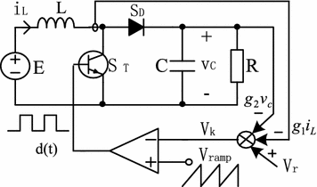
Boost regulator with proportional modulation
![$$G_{0} (p) = \left[ {\begin{array}{*{20}c} p & {\tfrac{1}{L}} \\ {\tfrac{ - 1}{C}} & {p + \tfrac{1}{RC}} \\ \end{array} } \right],\quad G_{1} (p) = \left[ {\begin{array}{*{20}c} 0 & {\tfrac{ - 1}{L}} \\ {\tfrac{1}{C}} & 0 \\ \end{array} } \right]$$](../images/419194_1_En_5_Chapter/419194_1_En_5_Chapter_TeX_Equ62.png)
5.4.1.1 Find the Main Term of the Steady State Solution
![$${\mathbf{x}}_{0} = {\mathbf{a}}_{00} = [I_{00} ,V_{00} ]^{Tr}$$](../images/419194_1_En_5_Chapter/419194_1_En_5_Chapter_TeX_Equ63.png)

From Eq. (5.51) we can see that for the closed-loop Boost converter with the inductor current being contained in the feedback amounts, the solution of d0 needs to solve a cubic equation, which can be solved by the numerical method or the commonly used formula of the cubic equation. There may be multiple real-value solutions that meet the condition of d0. In this case, they need to be determined by the stability analysis method of the equilibrium point (see Chap. 9).
However, if only the output voltage feedback is available, for the Boost circuit with the linear PWM feedback control, the solution of d0 only needs to solve the quadratic equation. Thus under this condition it is easy to determine whether the solution meets the requirements of the converter, and it is also indicates that potential instability factors would exist in the closed-loop converter system with current feedback control.

Here  are independent of the switching frequency of the circuit, which is the same as the steady-state DC solution obtained by the state space method.
5.4.1.2 Find the First-Order Correction
![$${\mathbf{x}}_{1} = {\mathbf{a}}_{11} e^{j\tau } + {\bar{\mathbf{a}}}_{11} e^{ - j\tau } ,\quad {\mathbf{a}}_{11} = [I_{11} ,V_{11} ]^{Tr}$$](../images/419194_1_En_5_Chapter/419194_1_En_5_Chapter_TeX_Equ66.png)
![$$\begin{aligned} V_{11} & = \frac{{(b_{11} + b_{10} ) \cdot [j\omega L \cdot I_{00} - (1 - d_{0} ) \cdot V_{00} ]}}{{\omega^{2} LC - (1 - d_{0} )^{2} - j\omega L/R}} \approx \frac{{(b_{11} + b_{10} ) \cdot [j\omega L \cdot I_{00} - (1 - d_{0} ) \cdot V_{00} ]}}{{\omega^{2} LC - (1 - d_{0} )^{2} }} \\ I_{11} & = \frac{{(b_{11} + b_{10} ) \cdot V_{00} - (1 - d_{0} ) \cdot V_{11} }}{j\omega L} \\ \end{aligned}$$](../images/419194_1_En_5_Chapter/419194_1_En_5_Chapter_TeX_Equ67.png)

First-order ripple component of state variables and correction of duty ratio
Frequency |
|
|
|
|---|---|---|---|
fs = 50 kHz | −0.1372 − 0.0692j | 0.0589 + 0.1093j | −0.0656 |
fs = 100 kHz | −0.0742 − 0.0292j | 0.0437 + 0.0370j | −0.0325 |
fs = 1 MHz | −0.0078 − 0.0024j | 0.0053 + 0.0018j | −0.0032 |


Obviously  is inversely proportional to the switching frequency.
5.4.1.3 Find the Second-Order Correction


The final expression of the steady-state periodic solution can be obtained from Eqs. (5.51) to (5.57), as shown in Eq. (5.48a), in which the steady-state DC solution is  , i.e.,
  .
.
Steady-state solutions of state variables in example 1
Frequency | ESPM | Numerical simulation |
|---|---|---|
fs = 50 kHz | I0 = 0.3325A V0 = 6.9796 V | I0 = 0.3750A V0 = 7.0472 V |
fs = 100 kHz | I0 = 0.4253A V0 = 7.7490 V | I0 = 0.4430A V0 = 7.6504 V |
fs = 1 MHz | I0 = 0.5032A V0 = 8.3934 V | I0 = 0.5267A V0 = 8.3355 V |
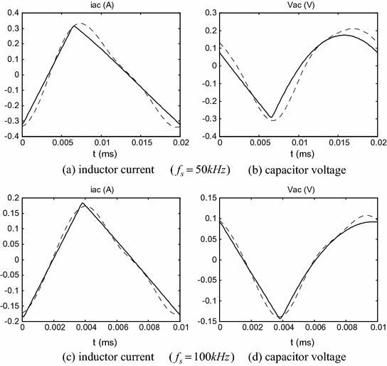
Steady-state ripples of state variables for Boost with proportional control
It can be seen from the data in Table 5.2 and the waveforms in Fig. 5.3 that the results obtained by the two methods are close, especially at higher frequencies. The difference is smaller, means that the ESPM introduced in this paper is effective. At the same time, it can be seen from Table 5.2 that when the switching frequency is low, the DC component has a certain change, which is called DC offset.
5.4.2 Boost Regulator with Proportional-Integral Control
Steady-state solutions of state variables
Frequency | ESPM | Simulation |
|---|---|---|
fs = 50 kHz | I0 = 0.5117A V0 = 8.4618 V | I0 = 0.5011A V0 = 8.2435 V |
fs = 100 kHz | I0 = 0.5115A V0 = 8.4617 V | I0 = 0.5166A V0 = 8.3137 V |
Fundamental components of the state variables and the 1-order correction of duty cycle
Frequency |
|
|
|
|---|---|---|---|
fs = 50 kHz | −0.1617 − 0.0431j | 0.0873 + 0.1032j | −0.00002 |
fs = 100 kHz | −0.0796 − 0.0223j | 0.0490 + 0.0336j | −0.000005 |


Steady-state ripples of state variables for Boost with PI control
It can be seen from the data in Tables 5.3 and 5.4, and the ripple waveforms in Figs. 5.3 and 5.4, that when there is a compensation capacitor in the feedback control circuit, the results from the ESPM agree quite well with those from numerical simulation, which means that the ESPM has a higher accuracy. The compensation capacitor makes the ripple have a very small effect on the duty cycle because of its filtering characteristics (see Table 5.4). Thus, the errors introduced by some of the assumptions made during the algorithm derivation are quite small.
5.5 Improvement of the Algorithm
5.5.1 Improved Algorithm for Duty Cycle Correction
According to the basic principle of the equivalent small parameter method, when the term di is solved, the items that are explicitly related to di are moved to the solution equation of higher order correction, so the right side of Eqs. (5.18a)~(5.18d) no longer contains the explicit relation with di, it is the linear equation of di.


![$$\begin{aligned} A & = K_{1} \cdot j2\pi (A_{1} - \bar{A}_{1} )a_{00} \\ B & = 1 + K_{1} \cdot j2\pi (A_{1} b_{10} \cdot e^{{j\tau_{s0} }} - \overline{{A_{1} b_{10} }} \cdot e^{{ - j\tau_{s0} }} )a_{00} + K_{1} \cdot (A_{1} + \bar{A}_{1} )a_{00} \\ D & = K_{1} \cdot (A_{1} b_{10} \cdot e^{{j\tau_{s0} }} + \overline{{A_{1} b_{10} }} \cdot e^{{ - j\tau_{s0} }} )a_{00} \\ A_{1} & = [G_{0} (j\omega ) + d_{0} G_{1} (j\omega )]^{ - 1} \cdot G_{1} (j\omega ) \\ \end{aligned}$$](../images/419194_1_En_5_Chapter/419194_1_En_5_Chapter_TeX_Eque.png)
Obviously, according to (5.59), there would be more than one solution for d1, thus the correct value of d1 needs to be selected according to the actual situation of the system.
![$$\begin{aligned} a_{02} & = - [G_{0} (0) + d_{0} G_{1} (0) + G_{1} (0) \cdot K_{1} \cdot a_{00} /C_{1} ]^{ - 1} \cdot G_{1} (0)(B_{1} + a_{00} \cdot B_{2} /C_{1} ) \\ d_{2} & = (K_{1} a_{02} + B_{2} )/C_{1} \\ \end{aligned}$$](../images/419194_1_En_5_Chapter/419194_1_En_5_Chapter_TeX_Equ76.png)
![$$\begin{aligned} B_{1} & = (b_{11} + b_{10} )\bar{a}_{11} + (\bar{b}_{11} + \bar{b}_{10} )a_{11} + d_{1} a_{00} \\ B_{2} & = K_{1} \cdot [2R(a_{22} e^{{j\tau_{s1} }} ) + 2R(a_{32} e^{{j\tau_{s1} }} )] \\ C_{1} & = 1 + K_{1} \cdot [4\pi \cdot I(a_{11} e^{{j\tau_{s1} }} ) + 8\pi \cdot I(a_{22} e^{{j\tau_{s1} }} ) + 12\pi \cdot I(a_{32} e^{{j\tau_{s1} }} )] \\ \end{aligned}$$](../images/419194_1_En_5_Chapter/419194_1_En_5_Chapter_TeX_Equf.png)
5.5.2 Correction Algorithm for Series Expansion of the Switching Function δ(t)


In this way, the series expansion form of the switching function in the closed-loop converter system is unchanged, and the process of solving is exactly the same as the original algorithm, except that the coefficients of some items would become zero, for example b21 = 0, b31 = 0.
5.5.3 Double Iterative Symbol Algorithm
In order to distinguish the algorithm to be proposed below, we refer to the algorithm of the closed-loop system proposed in Sect. 5.4 as the single-iteration symbol algorithm (or basic algorithm).

However, it can be found from the expansion of δ in (5.32a) that in the closed-loop solution, a portion of the DC component in (5.63) is shifted to higher order equations for solution because of the duty cycle and the steady-state periodic solution are both expanded into the sum of the main term and the small correction terms. Similarly this is also the case in the solution of other components. Thus, it is possible to achieve a higher accuracy by using single-iteration symbol algorithm to iterate several times.
When the equivalent small-parameter method is adopted, since the influence of the higher harmonics on the duty ratio is small, it can be considered that when solving the steady-state periodic solution of the closed-loop system, the duty ratio has been determined after three iterations, that is, d = d0 + d1 + d2, is considered to be constant. In order to improve the convergence speed, the system can be solved once again by the equivalent small parameter solution method of the open-loop system. This method of solving the closed-loop system of the switching power converter first, after determining the duty ratio, considering the system as an open-loop system, and then solving it again with the ESPM is called double iterative symbol method.

 is the same as before. According to equations from (5.23) to (5.29) on the method of dividing the integral interval, there are:


 in (5.32a), the value of the following coefficients is zero, i.e., b11 = b12 = b21 = b22 = b31 = b32 = 0, and the coefficient bm0 is determined by

It can be seen that the first three terms of the series expansion of  are exactly the same as those of the open loop, which shows that the joint of the closed-loop solution method and the open-loop solution method are reasonable to determine the steady-state periodic solution of the closed-loop system.
![$$\begin{array}{*{20}l} {G_{0} (0)a_{00} + G_{1} (0)Da_{00} = u} \hfill \\ {[G{}_{0}(j\omega ) + G_{1} (j\omega ) \cdot D] \cdot a_{11} = - G_{1} (j\omega ) \cdot b_{10} a_{00} } \hfill \\ {[G_{0} (j2\omega ) + G_{1} (j2\omega )D]a_{22} = - G_{1} (j2\omega ) \cdot [b_{20} a_{00} + b_{10} a_{11} + b_{30} \bar{a}_{11} ]} \hfill \\ {[G_{0} (j3\omega ) + G_{1} (j3\omega )D]a_{32} = - G_{1} (j3\omega ) \cdot [b_{30} a_{00} + b_{10} a_{22} + b_{20} a_{11} ]} \hfill \\ {[G_{0} (0) + G_{1} (0)D]a_{02} = - G_{1} (0)(b_{10} \bar{a}_{11} + b_{10} a_{11} )} \hfill \\ \end{array}$$](../images/419194_1_En_5_Chapter/419194_1_En_5_Chapter_TeX_Equ86.png)
Note that when using the double iterative algorithm, the original closed-loop system needs to be decoupled, that is, the power stage main circuit is separated from the feedback compensation network, and only the main circuit state variables are solved. Since the duty cycle is considered constant at this time, the feedback network has no effect on the steady-state periodic solution of the power stage.
5.5.4 Analysis Example
Simulated results of state variables in different methods
fs | Methods | a0 | a1 | b1 | a2 | b2 | a3 | b3 |
|---|---|---|---|---|---|---|---|---|
50 kHz d0 = 0.4091 d1 = −0.066 d2 = −0.047 | B-ESPM | 0.3325 | −0.2744 | 0.1387 | −0.0587 | −0.0379 | −0.0013 | 0.0039 |
6.9796 | 0.1179 | −0.2186 | 0.0310 | 0.0407 | −0.0151 | −0.0052 | ||
I-ESPM | 0.3566 | −0.1938 | 0.13640 | −0.0649 | −0.0196 | −0.0040 | −0.0095 | |
7.0651 | 0.0332 | −0.1791 | 0.0372 | 0.0124 | −0.0084 | 0.0094 | ||
Numerical | 0.3766 | −0.2124 | 0.1349 | −0.0631 | −0.0289 | 0.0018 | −0.0071 | |
7.2230 | 0.0412 | −0.1994 | 0.0351 | 0.0237 | −0.0179 | 0.0070 | ||
Pspice | 0.3750 | −0.2295 | 0.1280 | −0.0643 | −0.0299 | −0.0073 | −0.0029 | |
7.0472 | 0.0571 | −0.1966 | 0.0294 | 0.0269 | −0.0145 | 0.0011 | ||
100 kHz d0 = 0.4091 d1 = −0.032 d2 = −0.022 | B-ESPM | 0.4253 | −0.1483 | 0.0584 | −0.0211 | −0.0210 | −0.0032 | 0.0069 |
7.7490 | 0.0875 | −0.0741 | 0.0098 | 0.0191 | −0.0014 | −0.0064 | ||
I-ESPM | 0.4287 | −0.1286 | 0.0606 | −0.0244 | −0.0188 | −0.0010 | 0.0036 | |
7.7465 | 0.0651 | −0.0698 | 0.0127 | 0.0153 | −0.0029 | −0.0030 | ||
Numerical | 0.4298 | −0.1295 | 0.0613 | −0.0247 | −0.0207 | −0.0009 | 0.0040 | |
7.7414 | 0.0641 | −0.0732 | 0.0127 | 0.0166 | −0.0049 | −0.0037 | ||
Pspice5 | 0.4430 | −0.1442 | 0.0481 | −0.0220 | −0.0222 | −0.0071 | 0.0053 | |
7.6504 | 0.0791 | −0.0669 | 0.0083 | 0.0169 | 0.0005 | −0.0066 | ||
1000 kHz d0 = 0.4091 d1 = −0.003 d2 = −0.002 | B-ESPM | 0.5032 | −0.0157 | 0.0048 | −0.0013 | −0.0020 | −0.0008 | 0.0009 |
8.3984 | 0.0107 | −0.0036 | 0.0008 | 0.0014 | 0.0005 | −0.0007 | ||
I-ESPM | 0.5023 | −0.0155 | 0.0048 | −0.0014 | −0.0020 | −0.0007 | 0.0009 | |
8.3856 | 0.0104 | −0.0036 | 0.0009 | 0.0014 | 0.0005 | −0.0006 | ||
Numerical | 0.5049 | −0.0156 | 0.0049 | −0.0014 | −0.0021 | −0.0008 | 0.0010 | |
8.3750 | 0.0106 | −0.0039 | 0.0009 | 0.0014 | 0.0005 | −0.0008 | ||
Pspice5 | 0.5256 | −0.0171 | 0.0031 | −0.0012 | −0.0019 | −0.0008 | 0.0008 | |
8.3348 | 0.0117 | −0.0035 | 0.0009 | 0.0011 | 0.0008 | −0.0008 |
The closed-loop Boost converter system in Sect. 5.4.1 is used as an analysis example. The basic algorithm of ESPM, the improved algorithm of ESPM, the numerical and the Pspice simulation methods are adopted respectively to analyze the Boost converter operated with different switching frequencies. The resulted DC component and the first three harmonic components of the state variables are listed in Table 5.5, in which a0 represents the DC component, ai and bi represent amplitudes of the cosine and sine components of the ith (i = 1,2,3) harmonic, respectively (see Eq. (5.48b)).
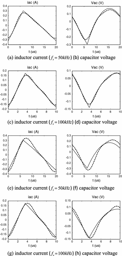
Comparison of simulated state ripple waveforms between numerical simulations and the ESPM (a–d: with the improved algorithm; e–h: with the original algorithm)
It can be seen from Table 5.5 and the waveforms in Fig. 5.5, that using the improved symbol algorithm to analyze the closed-loop switching power system can get more accurate results.
When the switching frequency is low and the ripple is large, the values of d1 and d2 in the direct ripple feedback control mode are larger. Therefore, when the single-iteration algorithm is used, the obtained DC component would have a larger error. However, this situation will be improved, and more accurate results can be obtained by using the improved symbol algorithm.
It can be seen from the above examples and Table 5.5, that the basic symbol algorithm can get more accurate results when the switching frequency is higher, or when the average feedback control law is used (i.e., the appropriate error compensation capacitor is added in the control loop to smooth the effects of ripples on the duty cycle). Because under these situations, the values of the first-order correction d1 and the second-order d2 are quite small, they have less influence on the duty cycle d.
5.6 Experiments and Verification
5.6.1 Diagram of the Experimental Circuit
 and
and  are the parasitic resistance and the current sensing resistor of the inductor respectively. In order to verify that the symbolic Equivalent-Small-Parameters (ESP) analysis method is still applicable in the case of high output ripple, we choose a lower switching frequency and a smaller output capacitance.
Experimental circuit of Boost regulator
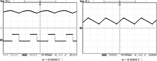
The TL494 PWM control chip is considered for experiments, its detailed internal block diagram, pin configuration and functions, and the operation principle can be found in related power integrated control circuit datasheet. The voltage of Pin-4 is used to limit the maximum width of the pulse, which determines the dead time control of the main circuit. The internal voltage reference  is provided by Pin-14. The resistors R3 and R4 set the reference of about 2.5 V on the negative input port (Pin-2) of the error amplifier (EA), and the output voltage of the main circuit is divided by resistors R1 and R2, setting the sampling voltage on the positive input port of the error amplifier (Pin-1). The error amplifier compares and amplifies the difference between the sampled and the reference voltage, and the resulted output error voltage is then compared with the sawtooth wave voltage signal of a constant frequency to generate a pulse with a certain width (the width of the pulse is directly determined by the error voltage). The pulse is shaped and amplified by TL-494 and then output via Pin-8, Pin-9 or Pin 10 and Pin-11 with a certain drive capability to turn on the power switch. Pins 5 and 6 are connected to the capacitor C6 and the resistor R9 respectively, which determine the oscillating frequency of sawtooth wave, i.e.,
  . The oscillation amplitude of the sawtooth wave is given by the relevant datasheet or measured by Pin-5. The maximum and minimum values measured in the experiment are
  and
and  (see Fig. 5.7b below). Pin-3 is the output of the TL-494 internal error amplifier. It is connected to the non-inverting input (Pin-2) of the amplifier with a RC circuit for error compensation and the self-oscillation suppression. To increase the stability of the error-amplifier circuit, the output of the error amplifier is fed back to the inverting input port through a resistor R5.
 is the sum of the resistance of resistor
  and potentiometer P1 in Fig. 5.6, and C1 is the sum of C11 and C12 in Fig. 5.6.
a Diagram of feedback controlled circuit, b measured sawtooth ramp and switching signal waveforms
5.6.2 Comparison of Experiment, ESPM and Simulation for Open-Loop System
 in Fig. 5.6 has such a large value that it can be replaced with an open circuit when the circuit operates in steady state, which means it does not affect the dynamic characteristics of the circuit, so it was ignored in symbolic analysis. Thus the main circuit is considered to be a second-order circuit. Disconnect the point A in Fig. 5.6, and connect a constant voltage
  independent of the output voltage of the main circuit at point A, then the circuit is in open-loop operation. The experimental results are
  ,
,  ; the current sensing resistor of the inductor
  . According to Fig. 5.7, the output voltage
  of the error amplifier and the duty cycle
  can be calculated as:

 ,
,  , thus, the actual switching frequency and duty cycle would be
From the comparison of Eqs. (5.71)–(5.73), it can be seen that the measured values are close to the theoretically calculated values.

![$$\begin{aligned} {\mathbf{G}}_{0} (p) & = \left[ {\begin{array}{*{20}c} {p + \tfrac{{r1 + R_{s} }}{L}} & {\tfrac{1}{L}} \\ {\tfrac{ - 1}{C}} & {p + \tfrac{1}{RC}} \\ \end{array} } \right],\quad {\mathbf{G}}_{1} (p) = \left[ {\begin{array}{*{20}c} 0 & {\tfrac{ - 1}{L}} \\ {\tfrac{1}{C}} & 0 \\ \end{array} } \right],\;{\mathbf{x}} = \left[ {\begin{array}{*{20}c} {i_{L} } \\ {v_{o} } \\ \end{array} } \right], \\ {\mathbf{u}} & = \left[ {\begin{array}{*{20}c} {E/L} \\ 0 \\ \end{array} } \right],\quad {\mathbf{f}} = \delta {\mathbf{x}},\;\delta = \left\{ {\begin{array}{*{20}l} 1 \hfill & {0 \le t \le DT} \hfill \\ 0 \hfill & {DT \le t \le T} \hfill \\ \end{array} } \right. \\ \end{aligned}$$](../images/419194_1_En_5_Chapter/419194_1_En_5_Chapter_TeX_Equj.png)

 ,
,  .
.
Waveforms of capacitor output voltage and switching signal (left) and sensed inductor current signal (right) for open-loop Boost converter
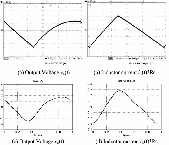
Comparison of state ripples for open-loop Boost converter: a and b measured results; c and d ESPM analysis (solid line) and Pspice simulation (dotted line)
Comparison of symbolic (ESPM) analysis, Pspice simulation and experiment for open-loop Boost converter
E = 18.30 V | DC values | Ripples | ||||||
|---|---|---|---|---|---|---|---|---|
|
|
|
| |||||
Max | Min | Amp. | Max | Min | Amp. | |||
ESPM | 0.8907 | 27.5296 | 0.2390 | −0.2493 | 0.4883 | 1.7654 | −2.4454 | 4.2108 |
Pspice5 | 0.8792 | 27.2668 | 0.2616 | −0.2783 | 0.5399 | 1.6904 | −2.8187 | 4.5090 |
Exp. | 0.9529 | 26.0 | 0.228 | −0.278 | 0.506 | 1.5 | −2.64 | 4.14 |


5.6.3 Comparison of Experiment, ESPM and Simulation for Closed-Loop System
![$${\mathbf{G}}_{0} (p) = \left[ {\begin{array}{*{20}c} {p + \tfrac{{r1 + R_{s} }}{L}} & {\tfrac{1}{L}} & 0 & 0 \\ { - \tfrac{1}{C}} & {p + \tfrac{1}{RC}} & 0 & 0 \\ 0 & {\tfrac{{m_{1} m_{2} R_{5} }}{{C_{1} }}} & {p + \tfrac{{m_{1} }}{{C_{1} }}} & { - \tfrac{{m_{1} m_{2} R_{5} }}{{C_{1} }}} \\ 0 & { - \tfrac{1}{{R_{2} C_{2} }}} & 0 & {p + \tfrac{{m_{3} }}{{C_{2} }}} \\ \end{array} } \right],\quad {\mathbf{G}}_{1} (p) = \left[ {\begin{array}{*{20}c} 0 & { - \tfrac{1}{L}} & 0 & 0 \\ {\tfrac{1}{C}} & 0 & 0 & 0 \\ 0 & 0 & 0 & 0 \\ 0 & 0 & 0 & 0 \\ \end{array} } \right],$$](../images/419194_1_En_5_Chapter/419194_1_En_5_Chapter_TeX_Equk.png)
![$${\mathbf{x}} = [\begin{array}{*{20}c} {i_{L} } & {v_{o} } & {v_{1} } & {v_{2} } \\ \end{array} ]^{{\prime }} ,\quad {\mathbf{u}} = [\begin{array}{*{20}c} {E/L} & 0 & {V_{R} R_{5} m_{1} /(R_{3} C_{1} )} & {0]^{{\prime }} } \\ \end{array} ,\quad {\mathbf{f}} = \delta {\mathbf{x}},$$](../images/419194_1_En_5_Chapter/419194_1_En_5_Chapter_TeX_Equl.png)


 is the duty cycle, which can be expressed as a linear function of state variable:

![$${\mathbf{K}}_{1} = [\begin{array}{*{20}c} 0 & {1 + m_{1} m_{2} R_{5} R_{6} )} & { - R_{5} m_{1} } & { - (1 + m_{1} m_{2} R_{5} R_{6} )]/v_{u} } \\ \end{array}$$](../images/419194_1_En_5_Chapter/419194_1_En_5_Chapter_TeX_Equp.png)
 ,
,  .
.
 , the duty cycle calculated by symbolic analysis method is
  , one can see that the measured result and the analytic calculation are in a good agreement.
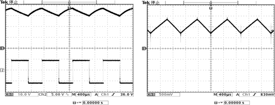
Waveforms of output voltage and switching signal (left) and sensed inductor current signal (right) for closed-loop Boost converter

Comparison of state ripples for closed-loop Boost converter: a and b measured results; c and d symbolic analysis
Comparison of symbolic (ESPM) analysis and experiment for closed-loop Boost converter
E 18.00 V | DC values | Ripples | ||||||
|---|---|---|---|---|---|---|---|---|
|
|
|
| |||||
Max | Min | Amp. | Max | Min | Amp. | |||
ESPM | 1.5146 | 34.7894 | 0.3733 | −0.3921 | 0.7654 | 3.2941 | −3.9366 | 7.2247 |
Exp. | 1.7142 | 33.7 | 0.318 | −0.344 | 0.662 | 3.28 | −3.96 | 7.24 |


5.7 Summary
In this chapter, the equivalent small parameter method (ESP) is applied to the steady-state analysis of the closed-loop converter system with CCM (continuous-conduction-mode) operation. A single-iterative and a double iterative symbol algorithm for analyzing the steady-state solution of the closed-loop system are proposed. It is shown that the equivalent small parameter method can be extended to the steady-state analysis of the closed-loop PWM switching converter system and still possesses the advantages of simple algorithm and high accuracy. The results are all analytical expressions, and from which the working mechanism of the circuit can be easily mastered. And moreover, the analytical expressions of the ripples would have obvious applications in the engineering design of circuit and computer symbolic simulation analysis.
In addition, the principle of the method and the analysis results in this chapter show that: (1) The effect of ripple on the duty cycle of the PWM closed-loop switching power converter system is quite small, especially at a higher switching frequency; (2) The DC offset presented in the system can be suppressed by adding the appropriate integral compensation in the feedback circuit; (3) The data comparison in Table 5.5 shows that using a single-iterative algorithm to analyze the closed-loop system with PI feedback control law has a higher accuracy (the actual application circuit is generally the case).
The comparison between experiments and the results of symbolic analysis further verified that the ESP symbol analysis method has high accuracy for the steady state analysis of open-loop and closed-loop systems of power switching converters even if the output contains large ripples.