NFV Infrastructure—Hardware Evolution and Testing
Abstract
In this chapter, we will look in detail at the architectural evolution in the Intel Architecture for NFV, including the increased dependence on cache efficiency for performance of NFV on CPU cores. We also look at the strategy of hardware augmentation that is opening the market for complimentary hardware acceleration through PCIE expansion. As with the software evolution in the preceding chapter, this leads to questions about our current architecture.
Keywords
Hardware evolution; Intel Architecture; NFV; CPU core; PCIE
Introduction
Enhancements and evolution in NFV performance are not limited solely to software. In the previous chapter, we focused on how certain software components, in cooperation with advances in hardware, have rapidly accelerated the performance of NFV systems, especially on commodity hardware. In this chapter, we will look more closely at hardware evolution and projections going forward in future generations of commodity hardware.
Starting with the expected Intel “tick/tock” delivery and evolution of processor architecture improvements and Network Interface Cards (NICs), hardware advancements to make Intel platforms perform at ever higher rates of throughput will create a parallel track toward NFV enhancement to the software technologies of virtualization we covered in Chapter 7, The Virtualization Layer—Performance, Packaging, and NFV.
In this chapter, we will look in detail at the architectural evolution in the Intel Architecture (IA) for NFV including the increased dependence on cache efficiency for performance of NFV on CPU cores. Intel is also pursuing a strategy of hardware augmentation that is opening the market for complimentary hardware acceleration through PCIE expansion. This expansion is further leading to next generation NICs that allow third-party chips to be embedded on those platforms, as well as the use of Field Programmable Gate Arrays (FPGAs) and Graphics Processing Units (GPUs) for similar purposes.
The compute model amenable to the existing IA, its execution and memory models (including cache behaviors) have downstream effects on programming/development models. If the pursuit of performance leads to true parallelism in compute architecture, hybrid models of the IA will appear or new models altogether. This might lead the reader to question how strong a grip Intel has on the NFV market as it evolves.
When combined with the variability in software architectures, the evolution of hardware architectures and accelerators results in an explosion of the number of testable permutations for NFV deployment.
One of the core contributions of the ETSI PER WG was the realization that an iterative methodology for bottleneck identification would be required, but a more open verification environment is overdue. So, before we leave performance, we will also touch on testability and how any performance claim for NFV can be tested objectively.
Evolving Hardware
All the interest around network I/O performance has its root in a basic truth about COTS compute (when NFV became a use-case of interest). That is, both COTS compute architecture and system design, while providing a flexible programming environment were not particularly optimized for network I/O (the word “compute” is a clue to where the real emphasis lies—processing power applied to general computation). The design is biased more toward minimizing latency than optimizing throughput. Thus the generic x86 Intel server1 (the presumed de facto NFV platform) needs some hardware tweaking and evolution to become a high-performance network appliance.
Just as we saw in virtualization software (via the use of vectors and shared memory transfers), there are a number of factors that can impact overall performance of a virtualized network function on existing CPU designs, including; I/O bandwidth, memory bandwidth/operations, processor operations, cache size (coherency and efficiency), context switching (data copying), the compute model (run to completion versus pipeline), multithreading, and coprocessing.
While it is possible to increase performance of the core pipeline (and system) by decreasing CPU cycle time (increasing frequency), optimizing instructions and applying a cache (all three are now in play in the IA) processor vendors have hit a ceiling on the first aspect (frequency).
Starting around 2003, increasing frequency started to show high cost (eg, increasing heat, error rate) and diminishing returns on performance (this process does not follow Moore’s Law for all operational parameters).2
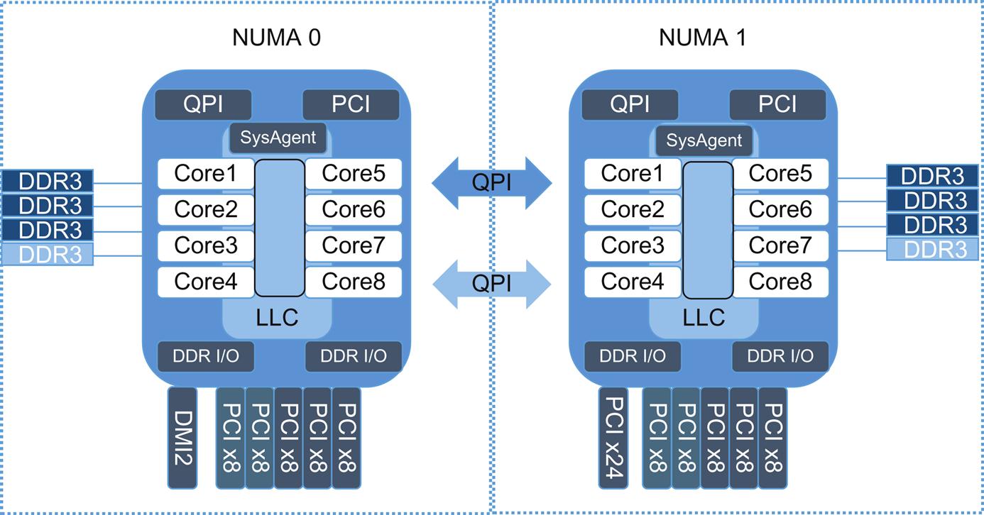
Instead of continuing to follow the steep/difficult processor speed curve, the approach to providing increased performance evolved into the creation of multiple execution pipelines and CPU manufacturers started making (generally lower clock speed) multicore and multisocket systems (exemplified by the Intel Sandy Bridge architecture shown in Fig. 8.1). This approach increases thread density and creates “some” hardware pseudo-parallel processing capability (although the underlying architecture and instruction set is still fundamentally designed for sequential execution and slowly adapting to exploit multicore).
CPU Complex
In the IA, work of a thread (a process with its own call stack and program counter) is accomplished through a series of instruction and data fetch, decode, execute, and store actions.
Within a shared memory multiprocessor system, multiple threads can operate concurrently on different processor cores, or on a single core (via scheduler interleaving). These threads transform the sequential execution model to a concurrent one, but with added complexities (in part, due to the fact that they share memory/state).
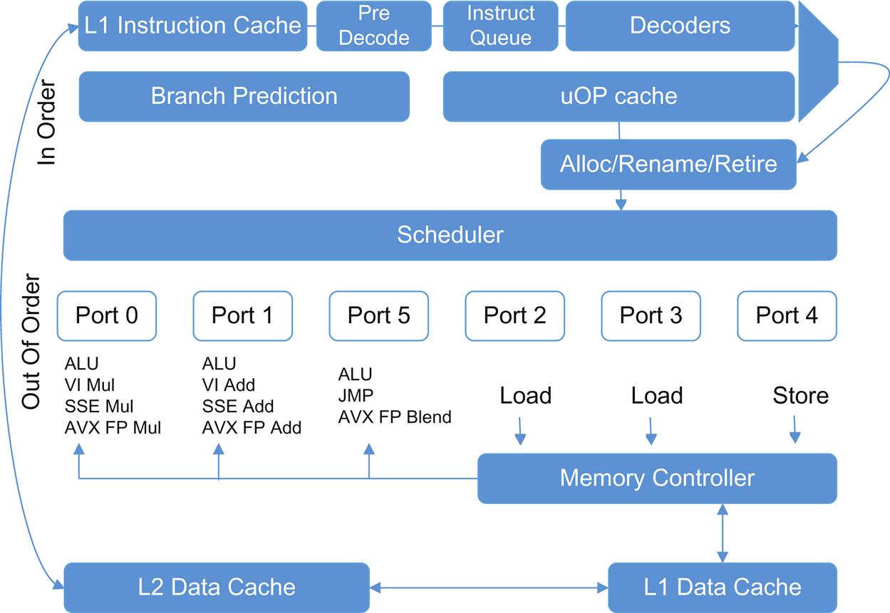
On a single core, the Intel Sandy Bridge microarchitecture (shown in Fig. 8.2) can support the simultaneous execution of multiple nondependent operations (eg, one load, one store, one AVX floating point multiply). The scheduler supports multiple entries in two clusters of “ports.” One cluster (the memory cluster) focuses on load/store operations allowing two simultaneous reads and one write per cycle (with an internal sequencer for queued requests) combined with masking these instructions.
On more recent platforms, another (the execution cluster) optimizes some instructions by “packing” (Advanced Vector eXtensions, AVX)3 into a larger operand size (256 bit), enabling (as an example) up to eight (32 bits) floating-point operations at a time (Single Instruction Multiple Data (SIMD) parallelism). As implied by the name, this is a vector strategy similar to the general packet buffer strategy covered earlier, but for arithmetic/floating-point instructions.
To maximize performance, the architecture supports hardware instruction pre-fetch and branch prediction (speculative execution). These speculative optimizations create instruction-level parallelism (ILP), but have penalties if they fail. These optimizations are algorithmic and depend on the loading conformance with predictive models. Because misprediction events have non-zero probability, recent changes in microarchitecture focus on increasing cache size and decreasing misprediction penalty.
If one of these optimized parallel instructions finishes before an earlier instruction, it will appear reordered4 (eg, multiple “load” instructions may continue to stack and execute in the timeframe that other operations run).
The external appearance of sequential execution (through visible state created by dependent instructions) is enabled by resources/structures that augment the scheduler—the reorder buffer (ROB), load/store buffers, and the physical register files (in the case of Sandy Bridge) for integer and floating point instructions. Given that load/store operations can also be reordered, the programmer bears the responsibility of using given memory fencing techniques and locking to maintain proper ordering which leads us down the very deep rabbit hole on maintaining concurrency in the face of parallelism. This is a heavy burden for a programmer and is also potentially error prone. It also can lead to very platform-specific code that may not be optimal on the next generation of the platform.
Note that use of AVX require orchestration awareness as to whether a generation of cores supports the instructions that may have been compiled into the application (an AVXv2 set is slated for release with the Haswell microarchitecture, Skylake introduces an AVXv3 set and we can expect further changes with successive ticks).
The Intel microarchitecture also exploits opportunities for further parallel instruction execution through simultaneous multithreading on the same core (hyperthreading).
Because hyperthreading depends on the sharing of critical core resources5 between threads it is most optimal when the threads access nonshared or noncontended for resources; otherwise one thread will block.
Like any virtualization mechanism, there will be a balance between full resource subscription and performance (that will vary from application to application). Resource oversubscription can have negative effects. If testing shows better performance for a function without hyperthreading, the operator might have some challenges in segregating out a subset of equipment with the feature turned off (this is currently a BIOS controlled feature and by default it is ON) specifically for the function.
By default, the scheduler has the flexibility to move threads between processor cores in a NUMA cell (an implicit optimization). This can have a negative consequence if the thread is depending on the use of local memory for high performance (cache).
Careful mapping of separate processes (and their threads) to cores (virtual or physical) can exploit the abundance of threads while minimizing conflict (at the core level).
Application and I/O processing can differ in application execution models (as depicted in Fig. 8.3)—run-to-completion or pipelining. The run-to-completion model is going to have an implicit requirement for flow load balancing to the cores associated with scale while the pipeline model can scale independent components.7
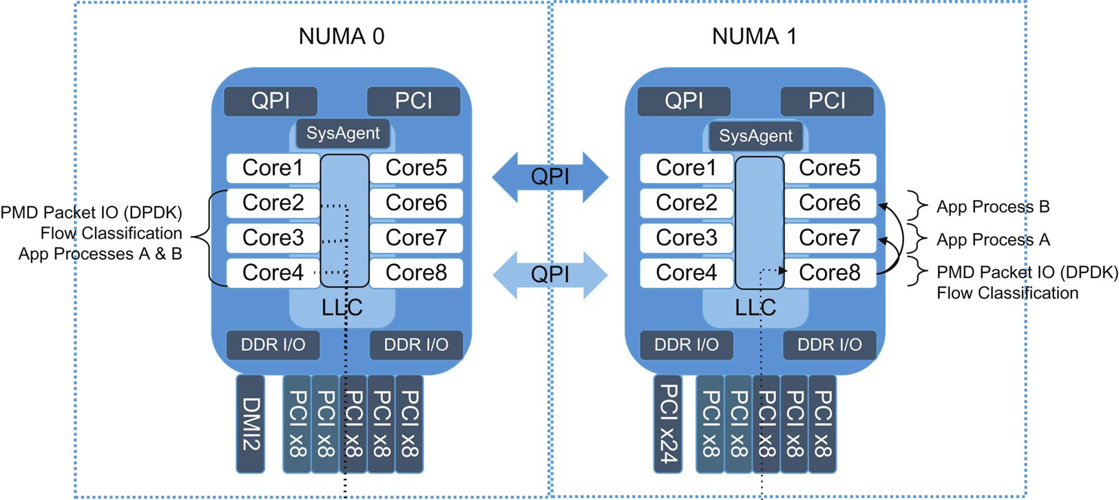
While it is possible to direct a flow to a core, “pinning” introduces load-balancing requirements and potential large flow HOL blocking problems.
At this point in time, another little-known effect is that the scheduler will still distribute kernel functions called by a pinned thread. Like all performance-related optimizations, this can be chased to yet another level. In this case, we will have to look at influencing the scheduler itself.
Individual programs can exploit these resources by becoming multithreaded and scaling across cores/threads.
Here, the complexity of the multisocket, multicore, paradigm percolates further up into design, development, and deployment by introducing concurrency management within the programs/applications (with compiler and CPU self-optimization dependencies).8
This assumes the individual program decomposes well into multiple concurrently running threads. Otherwise, enabling the ability to run more “copies” of the program may be beneficial, but the individual instances of the program might not be much more efficient.9 There are some design limits when we use “sequential, imperative code to implement a parallel algorithm.”10
While the multicore, multisocket paradigm (its accompanying instruction set architecture (ISA), cache and scheduler optimizations) provides some level of parallelism and resource sharing (through a combination of multithreading, SIMD, and ILP), performance inevitably suffers when the process has to actually access memory. While Intel has opened up bandwidth in memory access11 (memory technology has upgraded with every microarchitecture), latency is very hard to decrease for fundamental reasons.
Memory access—cache is king
The compute capacity is a function of the aggregate number of instructions per clock cycle across the cores working on a process.
While it is possible to spread some of this work out across multiple parallel operations, the thread run time efficiency will be dependent on avoiding/limiting memory accesses.
Today’s 10 Gbps network link has fairly strict service requirements. The smallest (64 byte) packets would arrive every 67 ns, and the larger (1518 byte) packets every 1230 ns12—effectively setting the timing/cycle budget for packet operations.
The typical router/switch vendor uses custom memories that optimize the small random access pattern (Fig. 8.4) associated with packet operations (smaller than the typical cache line size of a generic CPU at a higher rate).14 Generally speaking, specialized Network Processing Units (NPUs) can perform over an order of magnitude more memory accesses per second than the current crop of general-purpose processors.

Even though memory technologies associated with IA, including the overall bandwidth and latency between CPU and memory, have been evolving,15 fetching data from off-chip memory is still expensive in CPU clock cycles. Reasonable performance here is (currently) approximately 500 M access/second which includes bus turnaround and statistical bank conflict—multiple banks increase the “width” of access as long as simultaneous accesses do not attempt the same bank at the same time (with a variable delay of 10–100 s of ns). Increasing the number of cores is (generally) going to increase the number of memory accesses and bandwidth requirement. Further, (generally), the more bandwidth (read) provided the greater the chance of conflict.
There is also a memory bandwidth effect due to packet processing. The nonoptimized flow for a packet would be from NIC to memory, memory to CPU and the reverse (assuming the same core handled RX and TX)—creating a memory bandwidth multiplier per operation.
At higher port speeds, with nonoptimized access to data in memory, it becomes untenable to maintain line rate packet processing (for our example 10 Gbps interface). Memory partitioning per CPU, pinning, etc. can optimize the access to soften the impact on aggregate memory bandwidth. And, IA is moving forward in subsequent “ticks” to increase the number of channels and introduce “better” (faster, more power efficient) memory. For example, Haswell will introduce an option to use DDR4 versus DDR3 memory.
However, external memory access is the greatest bottleneck for network I/O performance because the processor will generally stall (for hundreds of cycles) during these reads (strategies like hyperthreading and out-of-order execution can somewhat mitigate the impact of stalling).
Because of this, system design has moved to hierarchical chip caches (Fig. 8.5) and improving cache efficiency, mapping, and cache prediction.
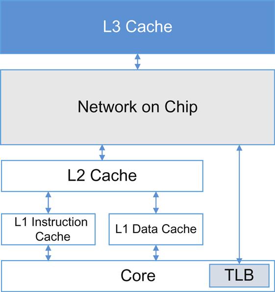
In comparison with external memory, the shared last level cache (LLC) can be accessed at a significantly lower latency: the rate of one cache line every 26 clock cycles (on average ~12 ns). The higher level caches operate even faster: L2 at 12 cycles (~3 ns) and L1 at 4 cycles (~1 ns or less with core pipelining). In general, the L1 cache can satisfy over a billion accesses per second with a variable (depending on cache state) but low latency.16
This is how we end up in the packet-handling scenario we painted earlier in the chapter. Optimizations17 attempt to tweak the microarchitecture in such a way that, optimistically, all operations (data/instructions) remain in cache (keeping the cache “warm”), and the architecture performs (theoretically) at the access rate of the LLC.
However, cache is still a limited and shared resource, and it too has its own optimizations. Smaller caches can be oversubscribed (eg, hashing of real memory to virtual memory can lead to cache-line contention) and certain behaviors (as well as “sharing” between cores and peripherals) can cause interference (eg, read/write-back cycles can clash between CPU and device in the case of peripherals writing directly into cache lines), resulting in cache evictions and thrashing.
The complexities of multicore architectures extend into the memory controller and ultimately the cache controller, because locality of memory to processing can dominate latency. While preferable over off-chip memory access latencies, larger caches can introduce latency (of their own) and other management/design problems. Yet, for network I/O-centric applications, that is the direction that system design is taking (in both general size and cache line width).
In a three-level cache (depicted), the lowest level cache is inclusive—shared amongst all cores. Algorithms that partition or “share”18 the cache to avoid interference between applications have been cropping up in academic research and have made it into the latest IAs.19 Hyperthreading may add some complexity to allocation (requiring a finer granularity of allocation: the current allocation maps a core to a QOS class).
Until cache allocation is pervasive and useful or perhaps in conjunction with it, Intel offers potential cache conflict mitigation through cache management software.20 Dynamic (external) resource monitoring and management (Intel proposes this in their SA architecture) enables management and orchestration entities to separate/isolate “noisy neighbors” (there is considerable academic research here as well on prediction and detection21).
As mentioned in Chapter 7, The Virtualization Layer—Performance, Packaging, and NFV, sharing of the LLC without hard partitioning introduces a number of security concerns when sharing in a multitenant environment.22
The layer 2 cache and the first level cache are specific to a core, but much smaller.23 Dependency on this locality is a reason to avoid dynamic reassignment by the scheduler.
Some improvements in DPDK performance (version 1.7 over version 1.6) are attributable in part to newer processor chips assigning a bigger portion of L1–L2 cache to I/O (and DDIO allows the NIC to write buffer descriptors to that cache24). This creates a high degree of cache locality and size dependency for performance.
Obviously, not all is perfect in the reliance on caching for NFV. There is also a concern, dependent on the cache architecture, that network flows directed to a set of cores (from a NIC) may have little commonality (broader hash) increasing cache miss probability (unless you increase the cache size). Additionally, the combination of too large a data set being loaded by an application thread with either too small a cache, too busy a cache, or a small cache partition, will push strain back onto the memory bandwidth itself (which currently cannot be partitioned).
Beyond the problems introduced in the large shared cache, maintenance of the private caches introduced in the expanding number of cores introduces coherency issues (where updates to data shared by multiple processors do not propagate quickly enough to avoid invalid/stale reads make it harder to maintain proper ordering of reads and writes). The result of these pressures has been cache coherence strategies (eg, directories, snooping, and snarfing25) that have evolved over time to reduce bus transactions between processors, invalidations, and other sharing side effects of the various algorithms.
Although some performance-impacting cache behavior can be mitigated through compiler optimizations or by fastidious data structure design by the developer, the growth of caches in IA imply a very tightly coupled overall system design (where “system” implies “socket” and everything on that socket, including the on-chip network connecting the socket resources and reliability components, like coherency controllers). Coherence protocols (overhead) can dictate performance-related changes in cache architecture.26
Cache coherency will continue to play a role in the realization of concurrency and the synchronization and appearance of serialization necessary for multithreaded application design (the presentation of a consistent memory model for the developer). The recent “tick”/generation (Haswell) introduces coherence improvements to realize a form of hardware transactional memory (transactional synchronization extensions, TSX). TSX provides an abstraction for atomic transactions that can potentially avoid some of the pitfalls of more granular lock-based mechanisms.27 As with almost everything we have talked about here, there are caveats in the use of TSX that might require additional optimizations.
Finally, beyond the simple system model (single socket) not all cache/memory access is the same—there is some concern around “locality” of memory. The QPI bus between sockets in the IA is a resource bottleneck for PCI traffic and NUMA node memory accesses.
A NUMA-unaware assignment of CPU resources (virtual and physical cores) to a VNF that straddles this bus will cause the application to be limited by the capacity and latency of the QPI bus.
PCIe—linking peripherals to the CPU
PCIexpress (PCIe) connections comprise the hardware path between peripherals, including accelerators and NICs and the CPU complex.
The current server and NIC market is comprised of a combination of older and newer PCI formats, splitting PCIe technology between version 2.0 and version 3.0 (Sandy Bridge EN/EP series now supports PCI 3.0).
The PCI SIG rates PCIe 2.0 at approximately 4 Gbps at 5.0 GHz28 clock rate (in each direction).29 PCIe 3.0 lanes are rated at approximately 8 Gbps.
The support for more/faster PCI connectivity has been scaling with the number of cores and sockets in the IA. For example, earlier versions of the Intel Xeon (E3—up to 10 cores in two sockets) supported 20 PCIe 2.0 lanes. The more recent E5(v2) versions come in two versions, 24 (EN) or 40 (EP) PCIe 3.0 lanes that could be configured in x4, x8, or x16 lane arrangements.30 In the PCIe 3.0 configurations (x8), Intel can currently map up to 16 physical functions onto 128 virtual functions.31
The dominant 10GE NICs in the market are (currently) 8 lane PCIe 2.0 and the newer entrants are 4 lane PCIe 3.0 (40GE NICs are shipping that are 8 lane PCIe 3.0 and 100 Gbps NICs are shipping that are 2×8×PCIe 3.0).
You really have to check the product literature for the controller to lane mappings. The E5v2 mappings are x4 on the DMI port (if you do not use DMI, it can be PCIe and they do not normally count these lanes in the total lane count). For most practical uses, there is (1) x8 lane and (1 or 2) x16 lane controllers, which can be subdivided logically further into 1, 2, or 4 ports (only on the 16 lane controller). This would set the maximum number of ports supported as well as their speeds—the ultimate limitation assuming you were going to use your PCIe bandwidth for no other peripherals.32
There is the potential to oversubscribe/undersubscribe the PCI bandwidth in a number of ways:
• A two-port 40GE NIC plugged into the 8 lane controller (PCIe 3.0) is technically oversubscribed (4 lanes or ~32 Gbps would be allocated to each port).
• A one port 100GE plugged into a controller would underuse the PCI bandwidth of a 16 lane controller (128 Gbps), while a two port would seriously oversubscribe.
Some vendors are attempting to work around these static limitations by making PCIe control more programmable. Solutions normally introduce more hardware to create the appropriate mappings between peripherals and processors.
In mix-and-match systems the PCI connectivity (eg, a PCIe 3.0 NIC in a 2.0 system or vice versa) is going to throttle to the PCIe 2.0 rate (least common denominator). So, misalignment of your NIC and platform capability can be a potential handicap.
Just like NUMA awareness is required in vCPU/cache optimization, intelligent traffic distribution to those structures also has NUMA dependencies (each socket has its own I/O hub that aggregates peripherals). Proper alignment of PCI termination (creating an orchestrated channel from the NIC to function) requires architectural awareness—to avoid inadvertent use of the QPI bus (in current IAs).
Even with the advent of PCIe 3.0, PCI bandwidth can become a performance limitation on current Intel-based platforms. Additionally, we should expect PCI technology to continue to evolve to match Intel’s product line.
In summary, performance claims may hinge on the availability and alignment of higher performance PCI technologies, and the introduction of PCI-connected accelerators may also stress this resource. PCI technology should see a next-gen evolution to keep in step with the changes in IA.
The bottom line for the digression into some of the hardware implications of the IA evolution is very basic—that Intel microarchitecture is on a constantly-changing course, including changes both subtle such as instruction set extensions, and profound including new memory technology, memory connectivity, cache size, upgraded PCIe support, inter-core connection, etc. Although other CPU vendors exist, the early dominance of Intel in NFV makes this easier (more documentation and available experience) to illustrate. We can by no means pretend that other microarchitectures are or will not follow similar trajectories. It is the fundamental awareness of this dynamic that is important to the discussion of NFV.
Extending the System
Assuming that there is a knee in the productivity associated with additional cores or larger caches (particularly for network I/O focused applications), the pursuit of performance (throughput) via the hardware path enters into the arena of system augmentation. Most recently, the use of specialized silicon on the NIC and/or coprocessors (both off and on die) has started to garner attention.
Network interface cards
Capable NICs (via their drivers) can take advantage of Receive-Side scaling (RSS). This process creates many hardware-based receive queues for inbound processing distributing traffic (and interrupt requests, though this may require some tuning of the IRQ affinity) intelligently across physical cores (this has proven to be less effective with virtual cores). RSS also provides load-balancing support into these queues (though not for all protocols).
Intel has specific enhancements that are available on their NICs, including (part of their I/OAT technology):
• QuickData Technology—an on-chip DMA engine that enables data copy by the chipset instead of the CPU, and moves data in the background.
• Direct Cache Access (DCA)—alluded to earlier, allowing a device (like the NIC) to place data directly into CPU cache.
• Extended Message Signaled Interrupts (MSI-X)—distributes I/O interrupts to multiple CPUs and cores (has to be evaluated in your environment).
• Receive Side Coalescing (RSC)—aggregates packets from the same TCP/IP flow into one larger packet, reducing per-packet processing costs for faster TCP/IP processing.
NICs can also support encapsulation/decapsulation offload processing, reducing the CPU load for these hypervisor/vSwitch-based operations. These include offloads for the TCP/IP stack, checksum calculation, large segment support for transmit and receive (that shift the segmentation burden to the NIC) and tunnel header processing.
Often overlooked, the ability to offload simple network functions like VXLAN encapsulation can improve throughput (looking forward, the offload for the IETF encapsulation for service function chaining will see similar benefits).
These capabilities can be combined to direct packets to the appropriate DMA queue, aligned with the appropriate CPU for a specific VM and eliminate the need for hypervisor-related processing on the receive side. QoS-based queuing or traffic prioritization obviously plays a role in avoiding HOL (head of line) blocking.
Some of the turnkey environments for NFV boast their own (purportedly superior) load distribution algorithms.
The range of potential NIC coprocessing/offloaded functions is large. Netronome,33 Cavium,34 EZChip,35 and Tilera36 offer 100GE (or multiple 10GE) capable NICs that perform more like a traditional hardware switch with dense onboard core sets that can offload forwarding lookups, session termination, encryption, and other functionality.
With the new generation of NIC acceleration, there is an attempt to entirely avoid handling packets with socket cores. Because these accelerators are not in the primary processing socket, they will likely have a different development cadence (than the processor cores).
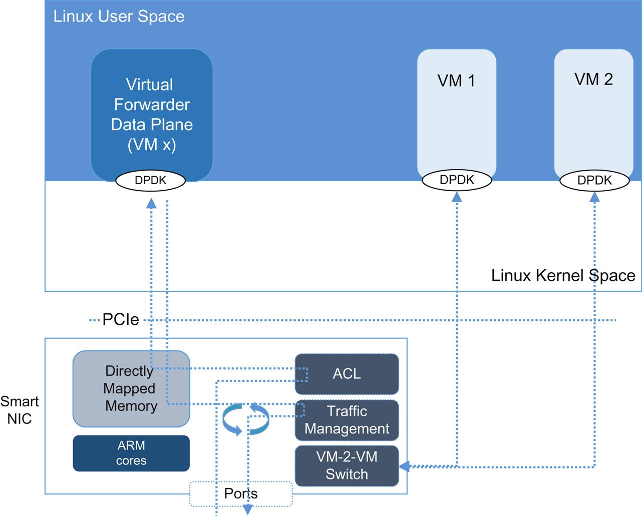
These NICs (generically depicted in Fig. 8.6) are essentially embedded NPUs.37 These vendors go to lengths to point out how limited core processors and sequential operation is for networking and how the migration toward heterogeneous cores (to provide parallelism) creates what their products already do (and how the data plane on the NIC and the control plane and application processing on the server CPU are more in tune with the SDN model).
With the number of cores they support (greater than 100 cores) they also pick on the need to dedicate cores for transmission management.
It seems natural that the smart NIC might be where dense, dedicated ARM cores might be leveraged against packet I/O processing. However, these solutions may not be restricted (over time) to use as an offload mechanism. EZChip has positioned its Tile-MX product line as not only an adapter but also as a standalone or blade-server NFV system (with hundreds of processors, they can support hundreds of VMs).
However, Intel is not staying still in the NIC market. They can (and will) integrate around their own switching silicon to create NIC appliance-like configurations with more offload(s), greater port densities and built-in hardware switching capabilities.
Heterogeneous cores
The multithreaded multicore processor designs of the IA with their large caches and superscalar (multiple instructions executed per cycle) or SIMD execution38 have limits in achievable parallel processing and diminishing returns as cores are added.39
Detractors of this design/paradigm think that it cannot continue and point to the memory access issues, inter-chip connectivity bandwidth and other bottlenecks as well as the diminishing returns due to an increasingly large instruction set (more compound operations), slow compiler advancement, and lagging application software efficiency (atomicity guarantees, concurrence management and adoption of newer instructions) as evidence; and ultimately to Amdahl’s Law.
A concerted effort has also gone into high-performance computation through the use of “dark,” heterogeneous, or specialized cores and processors; network hardware coprocessors for feature acceleration.
The fundamental idea behind early exploration began with the idea that a nonuniform distribution of chip resources for a more task-efficient allocation (and thus greater overall processor speedup).
The original examples for Intel QuickAssist (which foreshadowed the need for coprocessing) included the “usual suspects”—complex algorithmic functions like QoS traffic management and IPSec encryption. But the vision for application of these cores amongst competitors is much broader.
In the case of NFV applications, scalar/sequential and parallel processing might be combined within the application (parallelize what should be parallel).
FPGA and GPUs are emerging as candidates for these alternative cores.
Like the assets on the “smart” NIC, these offload engines will probably have to be virtualized. The techniques used depend on the technology. For the FPGA, the vFPGA will most likely be realized through static or dynamic resource partitioning and rapid context switching. The GPU resource grouping is closer to the existing/generic compute model and amenable to virtual execution contexts (but limited resources like load/store units need to be addressed).
Until they are integrated into the on-chip network, the FPGA and GPU will be addressed as PCIe peripherals. The limits of the PCI bus bandwidth will make them less attractive than other offload technologies.
Intel has proposed an expansion of the DPDK API to address hardware acceleration.40
Parallel processing may require rethinking algorithms and programming approach (identify parallelism in the code), addressing weaknesses in hardware/software of existing hyper-sequential approaches. The potential to gain from this approach has large dependencies on how amenable the network I/O processing task is to parallelization (percentage of the overall work that can be parallel, predictability of data access, cache friendliness) and the return over existing tooling like SIMD. But the aforementioned challenges of the hypersequential approach may make it attractive to explore alternatives.
Field Programmable Gate Array
Historically, FPGA technology has been expensive and development tooling has been an issue and barrier to entry for use in the general compute environment.
FPGAs have long been used in specialized networking hardware because of their performance/programmability combination (more readily software reconfigurable than microcoded NPUs or ASICs). They also have seen some adaptation in the area of high performance compute due to their utility in parallel processing (eg, high frequency trading, oil/gas exploration, and genomics).
It is this latter, complimentary processing role that has NIC vendors adding them today (discrete FPGAs)41 and CPU manufacturers planning put them into the socket (integrated) in the 2016 timeframe.
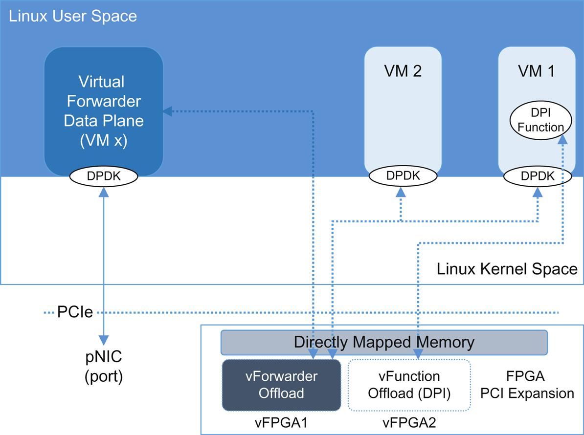
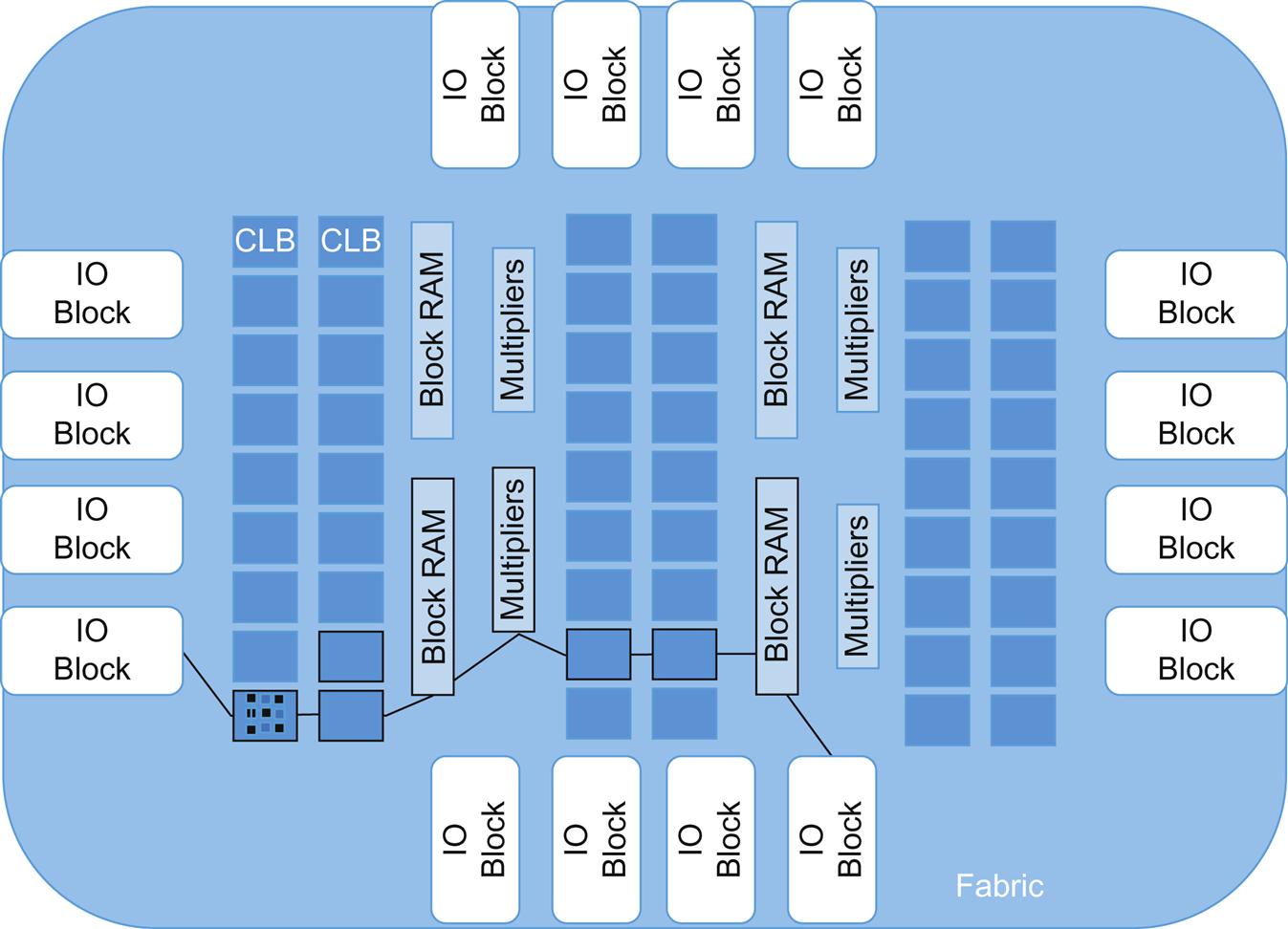
More than just a coprocessor, researchers are investigating the virtualization of the FPGA fabric as a shared resource (illustrated in Fig. 8.7).42 It is possible that it could replace the vSwitch or vforwarder functionality entirely as well as augment processing in VNFs. Communication can take advantage of most of the previously covered copy and context reduction technologies (DPDK shown).
The FPGA is a collection of memory and logical/computation cells (lookup tables and flip-flops) that can be composed into logic blocks, block RAMs (ie, storage), DSPs, and Etherent/PCIe communication/IO cores. While not particularly strong on floating point calculation (like the GPU or via the Intel AVX instructions a GPU), they do have some resources specifically for this sort of calculation. In these cases, range and precision are controlled since they affect chip area and memory bandwidth. FPGAs are now commonly packaged like a SoC (ie, a system on chip), combined with multiple ARM or other processors as a common fabric.
Multiple systolic arrays (kernels) are created across these resources that enable stream processing—multiple computational steps with minimal memory accesses (storing intermediate results—memory is distributed along with the logic blocks)—illustrated in Fig. 8.8.
The speedup comes from the number of simultaneous operations that can be done per clock time. The pipeline takes data in and does the first logical operation/action in the array (first logic cell or block) then recycles the intermediate result to the next cell/block for the next operation on next clock edge while new data is hitting the original cell/block. Typical “data machines” are several hundred logical blocks long and input/output can be across multiple pins, generating thousands of simultaneous operations once the pipeline is full.
Host memory provides source data. The accelerator is surrounded with shared memory for storing intermediate results between the accelerator and host, acting as a buffer. Memory choreography/synchronization is important and multiple incoming memory stream support is desirable.
Performance is a function of both the density (major vendors like Xilinx and Altera offer FPGAs with densities that exceed a million logical cells, thousands of DSP slices, support more than 50 Mbits of block RAM and implement enough transceivers to support multi-gigabit communication) of the cells/blocks and the efficiency with which the program is mapped to resources.43
FPGA acceleration is not automatic. The application is profiled to create a dataflow graph. From this, the compiler creates a dataflow machine used to reconfigure the FPGA. Dataflow machine size is limited by the size/area of FPGA, DRAM access, and pin bandwidth. Optimizations require a lot of effort and considerable tooling. Iteratively, successive dataflow graphs are generated and analyzed to derive a best fit on the available resources.
For a long time, the tooling required the use of specialized hardware description languages (Verilog, VHDL) and compilers and design was an art form. Recently, some vendors have come to market with higher-level language compilation and optimization support (eg, transforming runnable Java code into a data flow graph and optimizing that via kernel compilation to generate an FPGA structure44). These compilers can drive the orchestration of routine execution between a generic CPU (eg, Intel) running a specially adapted OS (eg, Linux) with a management program complement on the FPGA.
Nothing is static, and like the sequential processing solutions, FPGAs will also need to grow in capacity at a reasonable rate to provide more processing power.
In the end, the comparison of the ongoing growth cycles of CPU and FPGA technologies pits the growth in cell density of the FPGA versus core density growth of the CPU (at diminishing gains of clock rate). Similarly, it pits the dataflow mapping/special-compilation methodology of the FPGA versus the flow-mapping-to-core techniques and cache efficiency chase on the CPU. FPGA have advantages in power efficiency, particularly as the multicore paradigm has reached its efficiency “knee” (the point from which solutions take more power and generate more heat).
Integration of the FPGA in the CPU socket where FPGA is used as a heterogeneous core provides the mechanism for a synchronized tick/tock innovation cycle and eliminates a potential PCI bottleneck. Intel’s acquisition of Altera has already manifested by the inclusion of FPGA on die in some Xeon variants and is expected to ship in 2016. It remains to be seen if integrators will take advantage of it.
Finally, although new tooling exists for FPGAs, there is still limited choice. Solutions are still needed on the software development side to soften the cost of development and additional tooling.
Graphics processing unit
GPUs are potential accelerators and have been used in research like Packetshader.45 Like FPGA, they are used in High Performance Computing and have consumer applications (eg, gaming).
While the GPU was originally developed specifically for graphics processing (rasterization, shading, 3D, etc.), it has evolved to a more general-purpose programming model (GPGPU) that allows the GPU to be treated like a multicore processor (with an equally large, independent memory space). Many universities have curricula that include parallel programming techniques and include the use of CUDA,46 a domain-specific language for NVIDIA GPUs.
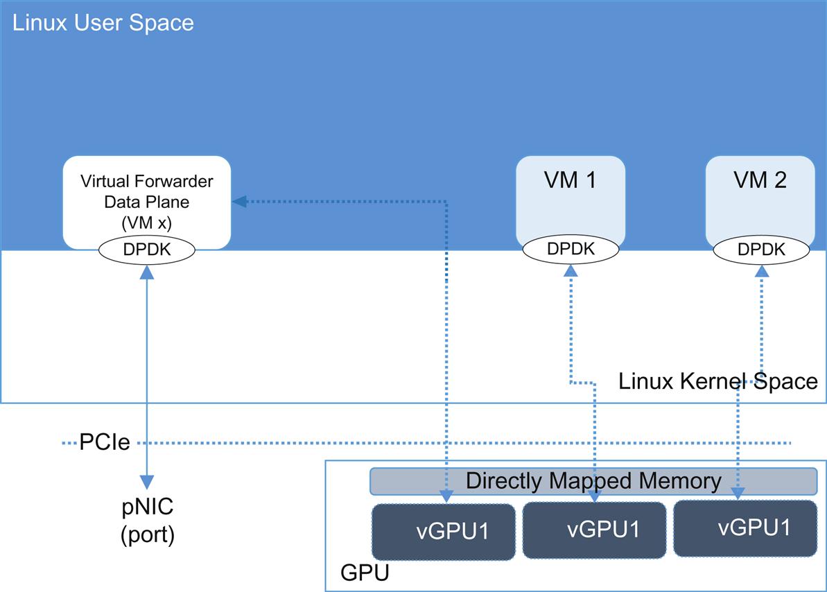
As generically illustrated in Fig. 8.9, the virtualized GPU processors could be directly mapped to VMs/containers possibly reducing their host resource requirements or used as standalone machines. Like the connectivity in the discreet FPGA, a number of copy/context saving mechanisms could be leveraged to provide access between the GPU and other cores. Most notably, this can result in the use of incoherent shared memory.47
Makers like NVIDEA48 and AMD49 offer products designed for more general compute tasks (parallel compute focus) with multiple streaming multiprocessors (SMs) on a die—each with 32 or more ALU (currently driving total core-equivalent density well into the hundreds)—illustrated in Fig. 8.10. Overall performance of these products is measured in many hundreds of GFLOPS (109 Floating Point Operations per Second). Be forewarned, not all GPU architectures are the same, even within the same manufacturer (they have application-focused designs).50
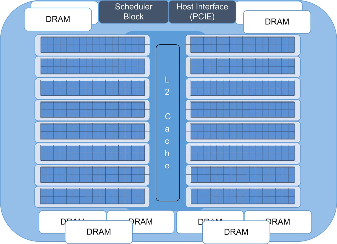
GPUs also use caching as arbitrage against memory access, though they currently are being designed with significantly greater memory bandwidth that may ultimately decrease this dependency.
As with the FPGA, SoC architectures with integrated GPP cores are emerging. (Intel’s Haswell has an integrated GPU with up to 40 “execution units.” Sandy Bridge and Ivy Bridge had models with up to 12 or 16 “execution units,” respectively.) This is still a much smaller size than is seen in designs mentioned earlier.
It remains to be seen if a large enough, on-socket GPU will evolve to be a serious network I/O off-load processor. Power consumption and resulting heat may make this a difficult design point. Until then, the use of the GPU as a PCI peripheral for this purpose will probably NOT be the best solution for this application because of limitations imposed both by PCI bandwidth and round-trip latency from NIC to GPU.
In addition, GPUs have also proven to be more difficult to virtualize/share than the cohort of competing technologies covered in this chapter.
The GPU cores are optimized for threads with long running series of computations and devote more area to this than is seen in the design of a generic processor architecture (lA).
Basic GPU programming technique creates a “kernel”—the computational component of an algorithm. Note that this is not the same concept as an OS kernel. Applications or libraries can have one or more “kernels.” After compilation, the “kernel” can be many threads, which execute the same routine. The threads can then be assembled into “blocks” of greater than a thousand threads, limited by scheduler capability to execute on an SM. This creates opportunities to share memory. In the case of NVIDEA, execution is in groups of 32 threads within the SM (ie, a “warp”)—even though in some cases, the number of ALUs in an SM is only 16 due to a higher clock rate for the ALUs. The GPU can also switch in and out of applications in tens of microseconds. All of which can be used to create large scale parallel processing such as multithreaded SIMD.
GPUs support their own ISAs and have their own unique development environments. These products support higher-level languages like C, C++, Java, and Python.
Heterogeneous compute challenges
Hardware diversity introduces complications, and a number of challenges emerge in heterogeneous compute environments, particularly tooling, core selection, and application steering (almost all of them borne by the developer).
From a tooling perspective, OpenCL51 is emerging as an API set and kernel specification for describing and programming heterogeneous compute models.
OpenCL is a very large idea; first, it is open source and second it is trying to provide a description language for multiple processor types. It is an abstraction of the underlying hardware.
For a developer, the chip manufacturer needs to stand up a product-specific OpenCL SDK, and a large number already have (NVIDIA, Altera, Intel).
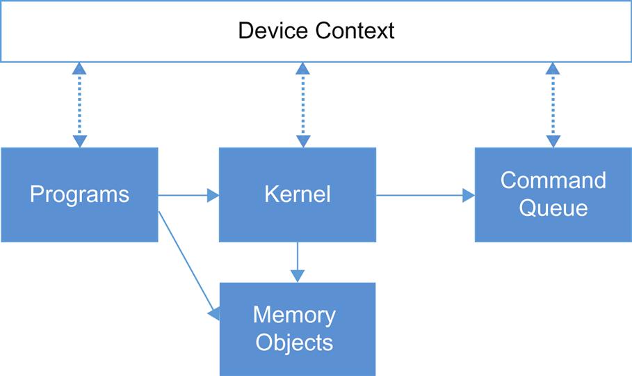
The OpenCL model (Fig. 8.11) starts with inventory of the OpenCL capable devices on the host creating what OpenCL dubs a “context.” Per-device programs are created, driven from the context associated devices. The basic unit of work is analogous to a function or the “kernel” in FPGA. These kernels are grouped as the equivalent of a program. OpenCL makes the analogy of a dynamic library with runtime linking.
Kernels are queued along with data transfers to different context elements for in-order or out-of-order execution. The individual kernel/functions are the equivalent of a thread and these can be grouped to create beneficial behaviors common to a “core” (eg, sharing local memory). OpenCL 2.0 allows the queueing control to be decentralized. OpenCL devices can queue kernels to themselves iteratively.
OpenCL also has to grapple with the concepts of shared virtual memory if and how the host and the accelerator pass data back and forth, language atomics support, and synchronization.
The kernel queuing above does raise some questions about scheduling optimization. Conventional thread scheduling is fairness/priority/affinity-centric in its algorithm(s). Some prior work is available around scheduling with monotonically increasing homogeneous processors such as different power/capability or the same ISA. That aside, with heterogeneous cores and accelerators, tasks will run on different processors with different efficiencies and modalities (SIMD or SPMD) requiring specialized processing distribution strategies.52 Some vendors outside of the OpenCL project are already suggesting “middleware”-like schemes for the SoC network to enable “demand scheduling.” Academic research is also beginning to investigate this problem.
There are some preliminary performance studies using OpenCL versus vendor-specific languages to program GPUs for a specific application such as video, but for a wider field of use performance has not been explored and what would be the basis for comparison. OpenCL cites a number of benchmark routines that leverage OpenCL, but the application is still largely video.
It remains to be seen if OpenCL will successfully address the development challenge in heterogeneous computing (programming for parallel processing requires not only new tools but an arguably different mindset/approach). They do boast support (via language extension, wrapper, compiler directive, etc.) in a number of tool chains, incorporation in a wide range of projects, and university-level courseware availability and adoption—all good signs of traction in the industry.
Nor is OpenCL the ONLY alternative here, as both OpenGL53 and OpenMP54 are attempting to promote their own communities with the same general ideas with slight variances in focus.
All the potential for tooling aside, it is unclear whether heterogeneity may still introduce software portability problems. It will certainly make scheduling more complex—even if we can overcome the first-order problem of effectively dividing the work into schedulable units.
There may also be some general/high-level impact from the use of heterogeneous cores and smart NICs on VM migration, which (for some) is required for NFV elasticity/HA. Similarly, upstream (orchestration) impacts on packaging and image management will also need to be ironed out.
In the end, further venture down this road might make the casual observer ask “aren’t you building a dedicated appliance … again?”
ARM
This chapter focuses primarily on IA based solutions. But, as noted earlier, there are other multicore CPU makers in the market.
The 64-bit ARMv855 (and accompanying ISA) has become a credible alternative, with many traditional CPU manufacturers developing ARM complements to existing products or ARM standalones.
This camp obviously backs the extension of COTS compute to do network services, but currently offers lower power consumption than the IA. The first commercial 8-core were touted by some to have a 50% greater power efficiency compared to equivalent Intel SoCs, but apples-to-apples comparison is difficult.56 ARM also offers what it markets as a better virtualization and security environment (TrustZone).
Hidden more deeply are architectural differences between ARM and Intel around concurrency with specific bearing on multicore systems. ARM supports a relaxed memory model that comes into play when multicore systems perform a “load” operation. The more-strictly-ordered Intel environment enforces a synchronization step between the cores to make sure one has not written to the cache location the load will access. Newer lock-free/wait-free algorithms can take advantage of the relaxed memory model of ARM, but do not have the same advantages on Intel.57 There are also subtle differences in core-interconnectivity (fabrics) and coherency strategies.
The potential problem with the use of ARM in NFV (and the complement or heterogeneous core environments just discussed) is the need to support two ISAs and their tool chains (for application developers). This may become less onerous over time as ARM is dominating in distribution of tablet computers, phones, and smaller devices—making the support of ARM development inevitable.
Linaro58 provides open source tools, compilers, and Linux support to ARM.
Turnkey (or “easy button”) deployment environments (eg, 6Wind) are also available for ARM.
ARM designs have the luxury of a large presence in non-server compute markets, particularly in smaller form-factor products like mobile phones and IoT devices, that allows them to continue to evolve a server solution competitive with Intel.
Performance Measurement
How can a vRouter vendor claim “120 Gbps of throughput per socket!” yet realize only 10 or 20 Gbps throughput on the multisocket server in your lab?
At a recent conference, an attendee asked a multivendor panel “is there any standardized measurement of performance for NFV?” By this point, the reader should realize how difficult the answer to that question might be. With the fluidity of virtualization architecture driven by ongoing software and hardware based network I/O evolution, there are multiple variables that can control the outcome. The latter evolution will directly affect the standalone performance of a service function, while the former will affect the performance of a service (multifunction). Further, depending on the evolution of metadata passing for SFC, specific services may perform better overall if the components pass metadata while that capability might be inconsequential to a standalone test.
It is not hard, however, to see why the answer is so desperately needed for consumers. Not surprisingly, prior to any real standards existing for NFV or SFC, vendors are already publishing performance claims for specific functions. As usual for our industry, these claims typically “hero” tests measuring port-to-port throughput without application operations—essentially, pipeline speed. In short order, as multiple vendors adopt the same virtualization methodologies, software tricks and base hardware, these claims all normalize except for some lingering and possibly purposeful ambiguity about how a vendor “counts” throughput.
So, how DO you measure performance?
Measuring Performance
Expectations for performance testing for virtualized service can get quite complicated.
However, establishing the formal testing methodology is the beginning of potential test work—as it can then be applied across a number of viable deployment permutations.
The test should start by aligning the physical and virtual resources appropriately for the microarchitecture (eg, avoiding NUMA and PCI problems).59 This consideration can be simplified somewhat by not fully loading the host (ie, “fully loaded” may be a separate scale test case).
The test permutations would include, roughly: the forwarder by itself, the VNF by itself, the forwarder and the VNF, a forwarder and multiple VNFs on the same host with parallel streams and a forwarder with multiple VNFs in a service chain. The virtual forwarder can be placed in the host or guest OS. There can be have multiple sometimes combined, acceleration techniques and virtualization environments (VMs, containers, hybrids).
A comparative test might also iterate through forwarders (eg, OVS, VPP, Snabbswitch60) and potentially multiple similar applications from different vendors. Should the test include service chains, the permutations of multiple vendor products would also have to be factored.
While it seems like the permutations are endless, by starting with an agreed-upon methodology, time and automation favor a solution. The very process of testing will eliminate or at least define the appropriateness of different permutations—and over time, noneffective ones will phase out (we learn more through comprehensive testing). The process will also end the period of wild but either inappropriate to deployment or unverifiable vendor performance claims.
The testing might be feature-, role-, or service-specific. Academic tests or shallow L2 port-in-port-out tests may not give an accurate view of performance and scale. Role-based tests are more expensive to craft and standardize, and agreed upon (existing) standardized role tests may need adaptation to a virtual environment.
Anecdotally, RFC 2544 methodology proved to be nondeterministic when applied to vRouter applications without some changes. It did this by showing a binary search in this context to provide maximum throughput for a specific loss tolerance and packet size. A methodology that extends RFC 2544 for NFV involves multiple runs that statistically smooth out behavior can lead to consistent results (eg, using a linear step method around worst/best measurements).
Numerous IETF proposals around this methodology exist. The vNet-SLA methodology proposed by Cisco Systems applies this idea (and was presented to OPNFV).61
A second round of problems will have to be addressed when comparing different hardware acceleration methodologies, once they become widely available.
This is a problem that directly confronts an organization like OPNFV, which they will attempt to pursue through their VSPERF work.
Meanwhile, several vendors have resorted to external testing for validation (Cisco and ALU have both gone to EANTC).62,63
Power Efficiency
Up to this point, there have been hints in the book that something unexpected might happen when an operator “switches to NFV” for their services. The unexpected impact is in power efficiency.
If the model for COTS compute for NFV is the general data center web application, then the operator might expect the average power consumption quoted for a particular server in that environment, where performance guarantees and power efficiency trade-offs, while orthogonal on the x86 platform are well understood.
The big difference for network I/O centric applications lies in the poll mode driver (as compared to an interrupt-driven mode) of some of the proposed performance enhancements. If you do not poll and use the built-in system power management (automatic frequency adjustment, idle sleep, etc.) the CPU clock will vary (eg, from 2.5–3.2 GHz to 400–800 MHz) and at very low clock rates, memory clocks may drop on some chipsets as well. Obviously, performance guarantees are no longer possible, but longer box life and lower power consumption are great trade-offs/compensations.
On the other hand, an implementation which operates strictly in poll mode, polls network devices constantly and feeds into a run-to-completion software stack which returns control to the poll loop until more data becomes available. Such an operation will consume the maximum power budget 24×7×365 by design and, for some designs, could exceed the maximum thermal limits of a rack, row or datacenter altogether.
Right now, relief in this paradigm is hard to find. Perhaps, it may be possible for the polling mode drivers (such as DPDK) to be enhanced to do the power management themselves (work in post 2.0 DPDK on the RX thread may provide opportunities), eg, reducing the CPU clock-speed and/or turning cores off based on multiple successive polls that return no data.
At first blush, adding GPUs and FPGA to an existing generic processor can also be expensive from a power perspective, but studies show that they are both more energy efficient for a unit of work.64 Both have power efficient operational modes (eg, hibernation) but could be as compromised as those in the generic processor unless the pipeline is empty. PCIE based cards can consume several hundred Watts, and directly adding FPGA/GPU will not make the generic CPU die operate any cooler. On-die accelerators will be a smaller form factor compared to their card-based counterparts with different overall capability and thermal impact. However, the longer impact may be more cost-efficient as the use of the GPU or FPGA could significantly decrease the number of required CPUs overall in a pure CPU environment.
Conclusion
It is a little ironic that the continuing cycle of hardware refresh that was the bane of network operations in the past, is now one of the accepted assumptions of anyone wishing to operationalize NFV or its related concepts. Hardware changes are thankfully less subtle than those in software. However, just as we saw with software enhancement for NFV, hardware enhancement needs to be quickly integrated into orchestration schemes and systems so that it is managed in operational environments appropriately. Resource management complexity needs to be managed in order to avoid recreating the equipment/inventory management challenges associated with the “dedicated appliances” environment that NFV is promising to replace.
The good news is that NFV has, and will continue, to motivate CPU vendors to push optimizations in cache design, additional core capacity including the number of sockets and cores per socket, new core types and internal communications bus technologies and strategies to address network I/O bottlenecks. NIC vendors similarly will continue to offer alternative or complimentary relief strategies including localized processing power offloads and hardware assists. Both traditional and new vendors may offer heterogeneous cores or exploit GPUs to achieve these continuously improving goals.
Our quick but detailed examination of the hardware evolution also leaves us with some questions:
• To repeat the question from the software performance chapter, will the economics really work for NFV when the power and cost of hardware performance enhancement are factored in? Are we factoring in the cost of continual integration of new/improved solutions?
• How is adding an I/O accelerator ultimately any different than building a dedicated appliance? If operators build a "Telco DC" full of I/O specialized platforms in support of NFV, how many variants are supportable before the idea of "theoretically substitutable infrastructure" mentioned in Chapter 2 is not recognizable?
• Will Intel be able to continue to evolve their architecture for NFV in a cost-effective way, or will the architecture splinter into a number of potential solutions (specialization)? If so, see the preceding questions.
• We need to focus on repeatable and standardized tests or benchmarks to assess performance/cost trade-offs and make accurate comparisons. Can OPNFV or some other forum provide an objective way to do this?
The overriding attraction of service creation, operational agility, and elasticity in NFV may still make the complications of performance enhancing specialization acceptable if it is pursued, and keep NFV attractive.
The proliferation of solutions today may also be a short-term problem as the market determines the proper optimization trade-offs going forward and/or as consumers opt again for the original NFV proposition by deploying only what is commonly available or nonspecialized. This may sacrifice some short-term potential performance (cost) for longer-term operational simplicity.
