Example: An Arduino Shield
In this chapter, you will learn how to use EAGLE to design a plug-in shield for the popular Arduino microcontroller board. The design will use a mixture of SMDs and through-hole devices. By following this example, you will learn how to design your own Arduino shields.
The example developed is for a four-digit, seven-segment LED display with a few extras in the form of a real-time clock chip, a piezo buzzer, and a rotary encoder. The shield could be used by those experimenting with making their own alarm clock or timer of some kind.
![]()
Figure 8-1 shows an Arduino Uno board. This is the most popular of the Arduino range of microcontroller boards.

FIGURE 8-1 An Arduino Uno.
The board has two rows of sockets on either side, and a wide range of plug-in shields are available that are the same size as the Arduino board but fit over the top of it and add extra features. Among other things, there are shields for Ethernet interfacing, controlling motors, and various kinds of displays.
![]()
When designing a shield, before wading into the schematic design, it is usually a good idea to think about exactly what the shield will do. In this case, we could set down the design goals of the shield as follows:
• A top shield; that is, no shields stacked on top of it
• Attractive design with retro four-digit, seven-segment display
• Real-time clock (RTC) chip
• Buzzer
• Rotary encoder with push switch
• Two-pin header output for connection to a relay module
![]()
Adafruit has created an EAGLE part for making a shield for the latest version of the Arduino Uno (the R3 at the time of writing). To use this, you will need to download and install the Adafruit EAGLE library. This is well worth doing anyway because there are lots of other useful things in the library.
If you did not install this library back in Chapter 1, then download the file adafruit.lbr from https://github.com/adafruit/Adafruit-Eagle-Library/blob/master/adafruit.lbr. Right click on the “Raw” button, and save the file to the .lbr folder in your EAGLE installation folder. You will then need to restart EAGLE.
![]()
Now that we have clarified what the board will do, create a new project (called TimerShield) and then a new schematic within the project also called TimerShield (see Chapter 2).
First, let’s add a letter-sized frame into which we can add our components. This step is obviously optional, but it does lend a certain air of professionalism to the design and is expected if you are going to be releasing the design to others, say, as an open-source hardware (OSH) design, as is the case for this shield.
You can find the frame part in the Sparkfun Aesthetics library, where it is called FRAME_LETTER. Use the Text tool to add some text over the “Design by” and “REV” fields. Before you drop the text over the field, change the layer in the Action toolbar to be layer “94 – Symbols.” You probably also want to set the font size using the “Size” dropdown in the Action toolbar.
My prefered way of designing a schematic is to first add all the key large components that I am going to need and then move and rotate them into well-spaced positions. I then add in all the smaller components such as resistors and capacitors.
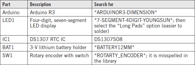
In this case, this means adding the components listed in Table 8-1 to the schematic.
TABLE 8-1 Key Components

After adding the components, set their names as shown in Table 8-1, and move them around and rotate them so that there is room for the extra components. Also add in the GND and 5-V power supplies. There are many of these in the libraries; I picked the ones from the Sparkfun Aesthetics library.
Aim for an arrangement that looks something like Figure 8-2.

FIGURE 8-2 Initial schematic with key components.
Turning our attention to the more minor components, there is going to be an NPN transistor for each of the cathodes of the four digits and accompanying base resistors. There will also be current-limitting resistors for each of the eight anodes, as well as the apostrophy and colon anodes.
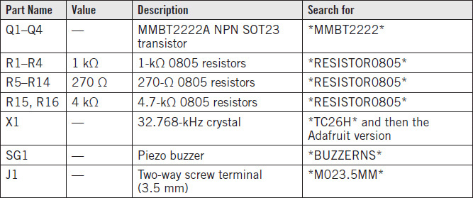
Add the components as listed in Table 8-2.
TABLE 8-2 Remaining Components

You will need to flip the transistors using the Mirror command so that they are facing the correct way around for the base to be closer to the Arduino. I also used the Smash command on the transistors to put the Name label closer to the symbol. Rather than add the four transistors using the Add command, it is quicker to add one transistor, mirror it, smash and move the label closer, and then use the Copy command to duplicate it three times. The same is true of the resistors of each value. So just add one resistor, set its value to 1 kΩ, and then copy it three times for R1 to R4, and then do the same for the other resistor values. Also change the values of the resistors as per Table 8-2.
When all the components are on the schematic, the design should look something like Figure 8-3.

FIGURE 8-3 All the components added.
We now just need to add all the nets to the schematic. For a schematic such as this, it is probably best to connect up the components in a certain area (perhaps around IC1) and until it looks like everything is connected that should be connected.
When working on a particular area, it helps to zoom in tight so that you can see what you are doing. Note that the display used is in real life slightly different from the library part. In fact, the colon and apostrophe LEDs have their anodes and cathodes swapped over. Thus, use Figure 8-4 as a reference. In Chapter 11, we will use this as an example of how you can modify a part.

FIGURE 8-4 Full schematic.
Once all the nets have been wired up, the schematic should look like Figure 8-4.
Sometimes, in a schematic, it is not practical to connect both ends of a net with a line. For example, in Figure 8-4, the link between the Arduino pin A0 and the buzzer, JP1, and the apostrophe cathode are a long way apart. I could have drawn a line between the two areas of the schematic, but instead I have used the Label tool. To do this, you need to
• Make both ends of the net be the same net by setting them to the same name with the Name tool. I called them A0 after the Arduino pin.
• Make a short length of net just going to a blank area on the schematic, where we are going to add a label. Do this for both ends of the net.
• Select the Label tool, and then click on the end of the net segments you have just made to add the labels.
We should also set up a couple of net classes to set desired track widths when we come to run the autorouter. Open the net class editor from the Edit → Netclasses menu item, and set the default netclass width to be 12 mils. Add another netclass (Nr 1) called “Power,” and set the width to be 24 mils (Figure 8-5).

FIGURE 8-5 Adding a netclass.
This is by no means essential, but given that if all the segements of one digit are lit, there could be over 100 mA flowing through the collector-emitter path of the transistors. Thus, to change the net class of the four nets that connect the collector of the transistor to DIG1 through DIG4 on the display, you also should set any GND net path to be of class “Power” too. The easy way to change these netclasses is to use the Change command, select “Class” and then “1 Power,” and then click on the nets you need to change.
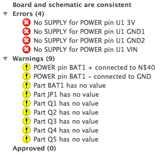
Having drawn the schematic, it’s time to run the electric rule checker (ERC). The result of this is shown in Figure 8-6.

FIGURE 8-6 ERC results.
At first sight, it seems like there are some things to worry about. But actually there aren’t. The errors referring to power supplies all spring from unmade connections to power on the Arduino. Because the Arduino is providing power to the shield, not the other way around, we can safely ignore these. None of the warnings are relevant either.
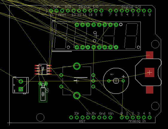
When you first select the menu option “Switch to Board,” the board layout that is subsequently generated will look something like Figure 8-7.

FIGURE 8-7 Initial layout editor mess.
As you can see, as well as the shield outline in the “Dimension” layer, there is also a default rectangular board area with the layout origin at its bottom-left corner. This rectangular board can be deleted and the Arduino shield board moved so that the origin is at its bottom-left corner.
We can now start dragging the components onto the board, starting with the display and rotary encoder, which we want to be fairly central to the board. We can also position the battery holder over to the right edge of the board, rotating it so that the battery can be easily replaced.
The same argument applies to the screw terminal, which is located on the left of the board where the other Arduino leads for USB and power are attached so that all the leads are on one side and easy to access.
While giving the key components their initial positions, we also need to consider what is going on beneath the board. For example, the Arduino Uno has a metal USB socket in the top-left corner (see Figure 8-1). So we do not want any through-hole leads immediately above that, which might make contact with the metal of the socket. The same applies to the center of the right-hand edge of the shield, where there is a six-pin ICSP header poking up from the Arduino. This is another reason why it is a good location for the surface-mount battery holder to be mounted on the top side.
With the key components positioned, the board will look something like Figure 8-8.

FIGURE 8-8 Key components positioned on the board.
We now need to drag on all the transistors and resistors. Because most of the “Digital IO” pins at the top of the board will have a resistor attached to them, drag over the appropriate resistors, positioning them under their input-output (IO) pin and rotating them as appropriate.
The transistors can be placed within the outline for the display. Because the display stands a little off the PCB, they can be on the top layer.
Figure 8-9 shows all the components on the board. Note that the air wires around the transistors seemed to be crossing over rather a lot, so they were rotated. It was also noticed that the buzzer has a polarity and that the positive (+) connection was currently to ground. The pins were swapped over in the schematic.

FIGURE 8-9 All the components on the shield.
We will add a ground plane to both the bottom and top layers. Remember, you do this using the Polygon tool, first setting the layer to “Bottom.” To get this to follow the shape of the board, you will also need to change the line style to a simple straight line rather than the normal orthogonal (right-angle) line style. This is next to the dropdown layer choice, once the Polygon command has been selected. Having drawn the polygon, use the Name command to set the name to be GND, and then hit the Ratsnest command to see the effect. Repeat this whole process but on the top layer. Because there are through-hole connections such as the GND connection of the screw terminal, there will automatically be a link between the two ground planes.
Run the autorouter, changing the routing grid to 25 mils before running. It should route 100 percent and produce a layout like that in Figure 8-10.

FIGURE 8-10 A routed layout.
We need to tidy up all the text on the board. We want any text that is to appear to be on the tPlace layer. So use the Smash command to separate all the labels from their parts, and then use the Change command to set the layer of the text that you want to keep to be tPlace.
Now use the Change command to make all the labels a Vector font and then set their size to 0.032.
Because this is an OSH project, we should also put the OSH logo on the board. This is a rare occasion where we can add a part to the Layout Editor rather than the Schematic Editor. Select the Add command, and then search for *OSH* in the component library and select the icon OSH-LOGO-L.
Also check for anything that is in the “tDocu” layer that you want to appear on the silk screen of the finished board. Because some parts such as the buzzer have their outline on the “tDocu” layer, we can just add the “tDocu” layer to the CAM job before we run it. We can also add some text for a URL next to the logo using the Text tool.
One of the problems with using an Arduino shield is that of documentation—knowing which of the Arduino pins are used and for what. A great place for this documentation is on the board itself, perhaps in the form of a little table. To draw this, it helps to set the grid to, say, 0.01 mil. Remember to set the layer of the lines to be “tPlace,” and a line width of about 0.05 mil will be about right.
We can check what will appear on the silk screen of the board by hiding all the layers except “tPlace” and “tDocu.” It is also useful to show “Pads,” “Vias,” and “Dimension” (Figure 8-11). The small cross marks next to each label will not appear on the final silk screen.

FIGURE 8-11 Checking the silk-screen appearance.
With a couple more labels added for JP1, the final board layout will look something like Figure 8-12.

FIGURE 8-12 Final board layout.
![]()
To generate the Gerber files for fabrication, we will use the Sparkfun CAM job that we saw in Chapter 6. However, having opened the CAM job, go to the “Top Silk Screen” tab and select the “tDocu” layer so that both the “tPlace” and “tDocu” layers are selected (Figure 8-13).

FIGURE 8-13 Selecting the “tDocu” layer in the CAM job.
The bounding rectangle for a shield board such as this is 2.7 × 2.1 in. (68 × 53 mm). If you shop around, you should be able to buy five boards for around $20.
![]()
If you are interested in making this shield, be aware that it is as yet untested. The LED display used has a manufacturer’s ID of TDCG1060M and is available from Mouser and Digikey.
In this chapter we have looked at designing an Arduino shield using EAGLE. In Chapter 9, we will look at another example project, this time building an interface board for the Raspberry Pi single-board computer.