PSpice, from MicroSim Corporation, is a computer program that can be used on many personal computers (PCs) for the analyses of electric circuits. PSpice is a derivative of SPICE which is a circuit simulation program that was developed in the 1970s at the University of California at Berkeley. SPICE is an acronym for Simulation Program with Integrated Circuit Emphasis. PSpice was the first derivative of SPICE that was suitable for use on PCs. PSpice and SPICE, which are similar in use, are both used extensively in industry. There are various versions of each.
Principally, only the creation of a PSpice circuit file (also called source file) is presented in this chapter. (But much of this material applies as well to the creation of a SPICE circuit file.) This creation requires the use of a text editor. Typically there are two text editors that can be used, one of which is in what is called the PSpice Control Shell.
The PSpice Control Shell is a menu system that includes a built-in text editor. The Control Shell can be run by simply typing PS at the DOS prompt (perhaps C: >), and then pressing the Enter key. After a few seconds, a menu appears. Menu items can be selected by using either the keyboard, mouse, or arrow keys to move horizontally and vertically within the menus. Running PSpice interactively using the Control Shell requires some study, at least for most PSpice users. The MicroSim Corporation has a User’s Guide that includes an explanation of the Control Shell, among many other features. And there are circuit analysis textbooks that explain its use. But no explanation will be given here.
Instead of editing via the Control Shell, some PSpice users may prefer to use an ASCII text editor, assuming one has been installed to be accessed from PSpice. In this case, the first step to utilizing PSpice might be at the DOS prompt to type CD PSPICE and then press the Enter key to change to the PSpice directory. Then, depending on the particular ASCII text editor, the next step may be to just type ED EEL.CIR and enter it. The ED is the code for edit, and EEL.CIR is the name of the circuit file. Another name such as EE.CIR is as suitable, but the extension. CIR must be included. Now the editing process can be begun and the circuit file created.
After the creation of the circuit file, the computer must be instructed to run the PSpice program with the particular circuit file. If the Control Shell is being used, then the Analysis menu item can be selected for doing this. If it is not being used, then all that is necessary is to type PSPICE followed by the name of the circuit file. The computer then runs the program and places the results in an output file that has the same name as the circuit file except that the extension. OUT replaces the extension. CIR.
Assuming no error notification, the final step is to print the output file. If the Control Shell is being used, this printing can be obtained via the Quit menu item. If it is not being used, then the printout can be obtained by typing PRINT followed by the name of the output file.
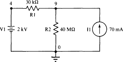
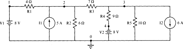
A specific PSpice circuit file will be presented before a general consideration of the basic statements. Below is the circuit file for the circuit of Fig. 7-1.
Fig. 7-1
In this circuit file, the first line, which is called a title line, identifies the circuit being analyzed. The last line is an.END line and is required complete with the period. The lines in between define the circuit, with one component per line. Each of these lines begins with a unique component name, the first letter of which identifies the type of component. Following each name are the numbers of the two nodes between which the component is connected. And following these node numbers is the electrical value of the component.
If PSpice is run with this circuit file, the following appears in the output file:
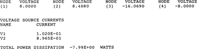
This printed output includes node voltages and voltage-source currents. The directions of these currents are into the first specified nodes of the voltage sources. The specified total power dissipation is the total power provided by the two voltage sources. Since this power is negative, these sources absorb the indicated 7.99 W. The E designates a power of 10, as often does a D in a SPICE output. In a SPICE output, though, the total power dissipation is the net power generated by all the independent sources, both voltage and current.
Now consider PSpice circuit file statements in general. The first line in the circuit file must be a title statement. Any comments can be put in this line. For future reference, though, it is a good idea to identify the circuit being analyzed. No other such line is required, but if another is desired, one can be obtained by starting the line with an asterisk (*) in column 1. Although not recommended, the title line can be left blank. But the circuit description (the component lines) cannot start in the first line.
Between the title line and the. END line are the component or element lines, which can be in any order. Each consists of three fields: a name field, a node field, and a value field. Spaces must appear between the fields and also between the node numbers within the node field. The number of spaces is not critical.
In the name field the first letter designates the type of component: R for resistor, V for independent voltage source, and I for independent current source. The letters do not have to be capitalized. Each R, V, or I designator is followed by some label to identify the particular component. A label can consist of letters as well as numbers, with a limit of seven in SPICE.
Each node field comprises two nonnegative integers that identify the two nodes between which the particular circuit component is connected. For a resistor, it does not matter which node label is placed first. For a voltage source, the first node label must be the node at which the voltage source has its positive polarity marking. For a current source, the first node label must be for the node at which the current enters the current source. Note that this node arrangement pertains when positive voltages or currents are specified, as is usual. If negative values are specified, the node arrangement is reversed.
As regards node numbers, there must be a 0 node. This is the node which PSpice considers to be the ground node. The other nodes are preferably identified by positive integers, but these integers need not be sequential.
The value field is simply the value—positive or negative—of the component in ohms, volts, or amperes, whichever applies. The resistances must be nonzero. Note that the values must not contain commas.
A comment can be inserted in a component line by placing a semicolon after the value field, then the comment is inserted after the semicolon.
As another illustration, consider the circuit of Fig. 7-2. A suitable circuit file is
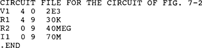
Fig. 7-2
In this circuit file, observe the use of suffix letters in the value field to designate powers of 10. The 2E3 for the VI statement could as well be 2K. Following is a complete listing of PSpice suffix letters and scale factors.
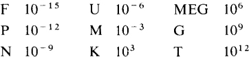
These suffix letters do not have to be capitalized; PSpice makes no distinction between uppercase and lowercase letters.
All four dependent sources are available in PSpice. Their identifiers are E for a voltage-controlled voltage source, F for a current-controlled current source, G for a voltage-controlled current source, and H for a current-controlled voltage source.
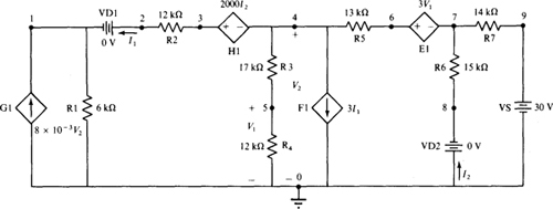
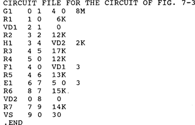
For an illustration of dependent source statements, consider the circuit of Fig. 7-3, and the corresponding circuit file below.
Fig. 7-3
In Fig. 7-3 the two “dummy” voltage sources VD1 and VD2, with zero in the value field, are needed because of the PSpice requirement that for a current to be a controlling quantity, it must flow through an independent voltage source. If no such source is present, then a “dummy” voltage source of zero volts must be inserted. The voltage is made zero to avoid affecting the circuit operation. The 0 need not be specified, though, because PSpice will use a default of 0 V.
For each dependent source statement, the first two nodes specified are the nodes between which the dependent source is positioned. Further, the arrangement of these nodes is the same as for an independent source with regard to voltage polarity or current direction.
For a voltage-controlled dependent source, there is a second pair of specified nodes. These are the nodes across which the controlling voltage occurs, with the first node being the node at which the controlling voltage is referenced positive. For a current-controlled dependent source, there is an independent voltage source designator instead of a second pair of nodes. This is the name of the independent voltage source through which the controlling current flows from the first specified node of the voltage source to the second. The last field in each dependent source statement is for the scale factor or multiplier.
PSpice does not have a built-in component for an ideal operational amplifier. From the model shown in Fig. 6-2b, though, it should be apparent that all that is required to effectively obtain an ideal op amp is a single voltage-controlled voltage source with a huge voltage gain, say 500 000 or more. If a nonideal op amp is desired, resistors can be included as shown in Fig. 6-2a.
So far, the only voltages and currents obtained have been node voltages and independent voltage source currents. Obtaining others requires the inclusion of a. DC control statement, and also a. PRINT statement in the source file.
If a circuit had, say, a 30-V dc voltage source named VI, a suitable. DC control statement would be

(VI was selected for purposes of illustration, but any independent voltage or current source can be used as a. DC control statement.) Note that two value specifications are necessary, which are both 30 here. The reason for having two of them is to allow for a variation in voltage. If, for example, three analyses were desired, one for VI = 30 V, another for VI = 35 V, and a third for VI = 40 V, the statement would be

where 30 is the first voltage variation, 40 is the last one, and 5 is the voltage increment between the variations.
Now, suppose it is desired to obtain the voltage on node 4 with respect to ground, the voltage across nodes 2 and 3 with node 2 referenced positive, the voltage across resistor R6 with the positive reference at the first specified node of that resistor, and the current through resistor R2 with the reference direction of the current being into the first specified node of that resistor. The required. PRINT statement would be

When a. PRINT statement is used, only the voltages and currents specified in that statement will appear in the output.
The DC must be included in the.PRINT statement to specify the type of analysis. Further, although optional, a DC specification is often included in each dc independent source statement between the node and value fields as in, for example,

With some versions of SPICE, only currents flowing through voltage sources can be specified as in, for example, I(V2). Also, voltages must be specified across nodes and not components.
PSpice requires a dc path to ground from each node. This is seldom a problem for dc circuits, but must be considered for some other circuits, as will be seen. Resistors and voltage sources (and also inductors) provide dc paths, but current sources (and capacitors) do not. A resistor of huge resistance can always be inserted between a node and ground to provide a dc path. The resistance should be large enough that the presence of the resistor does not significantly affect the circuit operation.
Each node must have at least two circuit components connected to it. This restriction poses a slight problem at an open circuit. One simple solution is to insert a resistor of huge resistance across the open circuit.
Finally, PSpice will not allow a loop of voltage sources (or of inductors). The insertion of a resistor in series with one of the voltage sources will eliminate this problem. The resistance should be small enough that the presence of the resistor does not significantly affect the circuit operation.
7.1 Repeat Prob. 4.11 using PSpice. Specifically, find the mesh currents I1 and I2 in the circuit of Fig. 4-14.
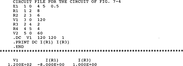
Figure 7-4 is Fig. 4-14 (redrawn and labeled for PSpice). Such a circuit will be referred to as a PSpice circuit. Following are the corresponding circuit file and the printed output obtained from running PSpice with this circuit file. Observe that I1 = I(R1) = – 8 A and I2 = I (R3) = 1 A are in agreement with the answers to Prob. 4.11.
Fig. 7-4
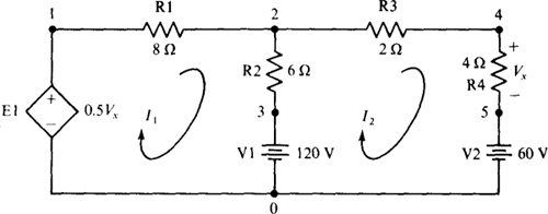
7.2 Repeat Prob. 4.15 using PSpice. Specifically, find the power absorbed by the dependent source in the circuit of Fig. 4-19.
Figure 7.5 is the PSpice circuit corresponding to the circuit of Fig. 4-19.
Fig. 7-5
Since PSpice does not provide a power output except for the total power produced by independent voltage sources, the power absorbed by the dependent source must be calculated by hand after PSpice is used to obtain the voltage across the dependent source and the current flowing into the positive terminal of this source.
In the following circuit file, observe in the V2 statement (V2 5 0 –16) that node 5 is the first specified node, which in turn means that the specified voltage must be negative since node 5 is not the positive node. Node 5 should be the first specified node because the controlling current Ix flows into it. Remember that a controlling current must flow through an independent voltage source.
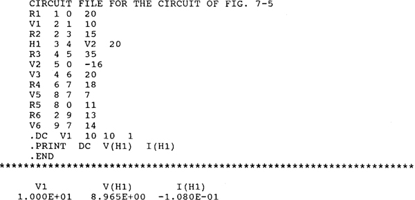
The power absorbed by the dependent source can be obtained from the printed output:

which agrees with the answer to Prob. 4.15.
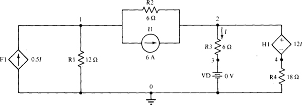
7.3 Repeat Prob. 4.22 using PSpice. Specifically, determine the current I in the circuit of Fig. 4-25.
Figure 7-6 is the PSpice circuit corresponding to the circuit of Fig. 4-25. This PSpice circuit, though, has an added dummy voltage source VD. It is the current in this source that is the controlling current for the two dependent sources. Again, remember that a controlling current must flow through an independent voltage source.
Fig. 7-6
Below is the corresponding circuit file along with the printed output obtained when this file is run with PSpice. The output I(R3) = 3 A agrees with the answer to Prob. 4.22.
7.4 Repeat Prob. 4.49 using PSpice. Specifically, determine the mesh currents I1 I2, and I3 in the circuit of Fig. 4-39.
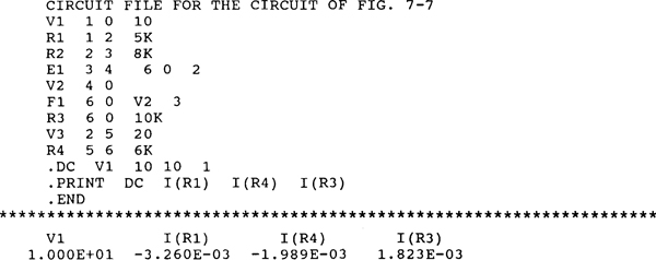
Figure 7-7 is the PSpice circuit corresponding to the circuit of Fig. 4-39. A dummy voltage source V2 has been included for the controlling current Ix to flow through.
Following is the corresponding circuit file along with the printed output obtained when this file is run with PSpice. The currents I (R1) = I1 = – 3.260 mA, I (R4) = I2 = – 1.989 mA, and I (R3) = I3 = 1.823 mA agree within three significant digits with the answers to Prob. 4.49.
Fig. 7-7
7.5 Repeat Prob. 5.11 using PSpice. In other words, obtain the Thévenin equivalent of the circuit of Fig. 5-20a.
Figure 7-8 is the PSpice circuit corresponding to the circuit of Fig. 5-20a. This PSpice circuit has a dummy voltage source VI inserted for sensing the controlling current I.
Fig. 7-8
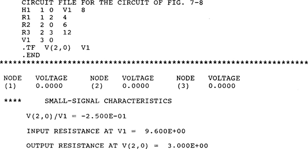
Above is the corresponding circuit file along with the PSpice output. In the circuit file a. TF statement has been included to obtain the Thévenin resistance. The format of this statement is

The resulting output consists of three parts:
1. The ratio of the output variable to the specified source quantity. For example, in the case in which the independent source provides an input voltage and the output is the output voltage, this ratio is the voltage gain of the circuit.
2. The second is the resistance “seen” by the independent source. It is the ratio of the source voltage to the source current flowing out of the positive source terminal with the other independent sources deactivated. In an electronic circuit, this resistance may be the input resistance.
3. The final output part consists of the output resistance at the terminals of the output variable, and includes the resistance of any resistor connected across these terminals. For the present case, this output resistance is the Thévenin resistance, which is the desired quantity.
The voltage gain and the input resistance parts of the output are not of interest. The printed output resistance of 3 Ω, the Thévenin resistance, agrees with the answer to Prob. 5.11. The Thévenin voltage is zero, of course, as is specified by the printed node 2 voltage.
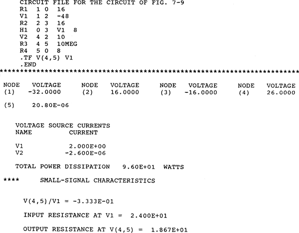
7.6 Repeat Prob. 5.46 using PSpice. Specifically, obtain the Thévenin equivalent of the circuit of Fig. 5-49 to the left of terminals a and b.
Fig. 7-9
Figure 7-9 is the PSpice circuit corresponding to the circuit of Fig. 5-49. A resistor R3 has been inserted across the open circuit at terminals a and b to satisfy the PSpice requirement that at least two components must be connected to each node. However, the resistance of R3 is so large that the presence of this resistor will not significantly affect the circuit operation.
Below is the corresponding circuit file along with the resulting output. A.TF statement has been included in the circuit file to obtain the Thévenin resistance. No .DC or .PRINT statements have been included because the node voltages will be printed out automatically. Observe that node voltage 4 is essentially the same as the voltage across terminals 4 and 5, the Thévenin voltage, because the voltage drop across resistor R4 is negligible. The obtained node 4 voltage value of 26 V and the output resistance value of 18.67 Ω, which are the Thévenin quantities, agree with the answers to Prob. 5.46.
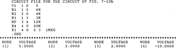
7.7 Repeat the first part of Prob. 6.13 using PSpice. Specifically, compute V0 in the circuit of Fig. 6-18.
Figure 6-18 is redrawn in Fig. 7-10a, for convenience. Figure 7-10b shows the corresponding PSpice circuit. Observe that the op amp has been deleted, and a model for it included. This model El is simply a voltage-controlled voltage source connected across the terminals that were the op-amp output terminals. The 106 voltage gain of this source is not critical.
Following is the corresponding circuit file along with the pertinent part of the output obtained when PSpice is run with this circuit file. Here, V0 = V(4) = —10 V, which is the same as the answer to the first part of Prob. 6.13.
Fig. 7-10
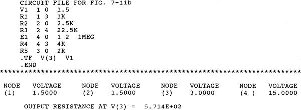
7.8 Repeat Prob. 6.20 using PSpice. Specifically, obtain the Thévenin equivalent of the circuit of Fig. 6-24.
Figure 7-1 la is the same as Fig. 6-24, and is included here for convenience. Figure 7-1 lb is the corresponding PSpice circuit in which the op amp has been replaced by a model El that is a voltage-controlled voltage source.
Below is the corresponding circuit file along with the pertinent portion of the output file. Node voltage V(3) = 3 V is the Thévenin voltage, and the output resistance of 571.4 Ω is the Thévenin resistance. Both values agree with the answers to Prob. 6.20.
Fig. 7-11
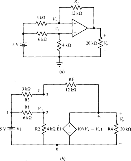
7.9 Repeat Prob. 6.24 using PSpice. Specifically, obtain the voltages V10 and V20 in the circuit of Fig. 6-28.
Figure 7-12a is the same as Fig. 6-28 and is included solely for convenience. Figure 7-12b is the corresponding PSpice circuit in which the two op amps have been replaced by models El and E2, which are voltage-controlled voltage sources.
Following is the corresponding circuit file and the pertinent part of the output file. The results of V(3)= V10 = 12.5 V and V(4) = V20 = 1 V agree with the answers to Prob. 6.24.
Fig. 7-12
7.10 Use PSpice to compute Ix in the circuit of Fig. 4-28.
Ans. –0.333 A
7.11 Use PSpice to determine I in the circuit of Fig. 4-45.
Ans. –3.53 mA
7.12 Use PSpice to find the Thévenin voltage at terminals a and b in the circuit of Fig. 5-44. Reference VTh positive at terminal a.
Ans. 143.3 V
7.13 Use PSpice to obtain V0 in the circuit of Fig. 6-21.
Ans. 10 V
7.14 Use PSpice to find V0 in the circuit of Fig. 6-22.
Ans. –1.95 V
7.15 Use PSpice to determine V10 and V20 in the circuit of Fig. 6-42.
Ans. 1.6 V, 10.5 V
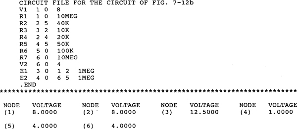
7.16 Without using PSpice, determine the output corresponding to the following circuit file.
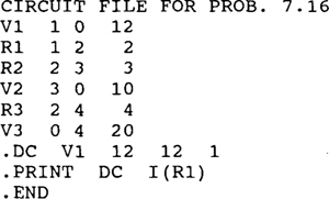
Ans. 4 A
7.17 Without using PSpice, determine the output corresponding to the following circuit file.
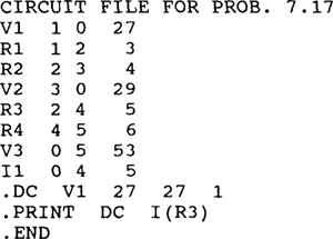
Ans. 4 A
7.18 Without using PSpice, determine the output corresponding to the following circuit file.
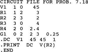
Ans. 6 V
7.19 Without using PSpice, determine the output corresponding to the following circuit file.
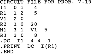
Ans. 1.6 A
7.20 Without using PSpice, determine the output corresponding to the following circuit file.
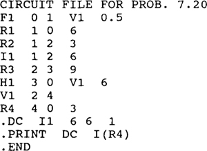
Ans. 3 A
7.21 Without using PSpice, determine the output corresponding to the following circuit file.
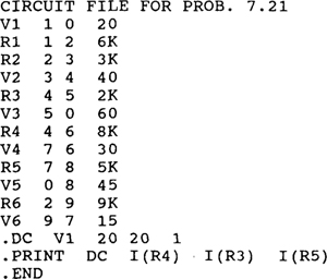
Ans. I(R4) = 6.95 mA, I(R3) = –14.6 mA, I(R5) = 10.0 mA
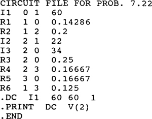
7.22 Without using PSpice, determine the output corresponding to the following circuit file.
Ans. –2V
7.23 Without using PSpice, determine the output corresponding to the following circuit file. (Hint: Consider an op-amp circuit.)
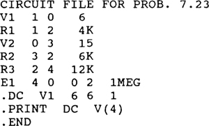
Ans. 12V
7.24 Without using PSpice, determine the output corresponding to the following circuit file. (Hint: Consider an op-amp circuit.)
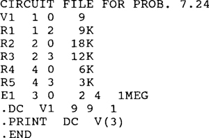
Ans. 12V