
This Springer imprint is published by Springer Nature
The registered company is Springer Science+Business Media LLC
The registered company address is: 233 Spring Street, New York, NY 10013, U.S.A.
This is not your father’s, your mother’s, or your grandparent’s Scanning Electron Microscopy and X-Ray Microanalysis (SEMXM). But that is not to say that there is no continuity or to deny a family resemblance. SEMXM4 is the fourth in the series of textbooks with this title, and continues a tradition that extends back to the “zero-th edition” in 1975 published under the title, “Practical Scanning Electron Microscopy” (Plenum Press, New York). However, the latest edition differs sharply from its predecessors, which attempted an encyclopedic approach to the subject by providing extensive details on how the SEM and its associated devices actually work, for example, electron sources, lenses, electron detectors, X-ray spectrometers, and so on.
In constructing this new edition, the authors have chosen a different approach. Modern SEMs and the associated X-ray spectrometry and crystallography measurement functions operate under such extensive computer control and automation that it is actually difficult for the microscopist-microanalyst to interact with the instrument except within carefully prescribed boundaries. Much of the flexibility of parameter selection that early instruments provided has now been lost, as instrumental operation functions have been folded into software control. Thus, electron sources are merely turned “on,” with the computer control optimizing the operation, or for the thermally assisted field emission gun, the electron source may be permanently “on.” The user can certainly adjust the lenses to focus the image, but this focusing action often involves complex interactions of two or more lenses, which formerly would have required individual adjustment. Moreover, the nature of the SEM field has fundamentally changed. What was once a very specialized instrument system that required a high level of training and knowledge on the part of the user has become much more of a routine tool. The SEM is now simply one of a considerable suite of instruments that can be employed to solve problems in the physical and biological sciences, in engineering, in technology, in manufacturing and quality control, in failure analysis, in forensic science, and other fields.
The authors also recognize the profound changes that have occurred in the manner in which people obtain information. The units of SEMXM4, whether referred to as chapters or modules, are meant to be relatively self-contained. Our hope is that a reader seeking specific information can select a topic from the list and obtain a good understanding of the topic from that module alone. While each topic is supported by information in other modules, we acknowledge the likelihood that not all users of SEMXM4 will “read it all.” This approach inevitably leads to a degree of overlap and repetition since similar information may appear in two or more places, and this is entirely intentional.
In recognition of these fundamental changes, the authors have chosen to modify SEMXM4 extensively to provide a guide on the actual use of the instrument without overwhelming the reader with the burden of details on the physics of the operation of the instrument and its various attachments. Our guiding principle is that the microscopist-microanalyst must understand which parameters can be adjusted and what is an effective strategy to select those parameters to solve a particular problem. The modern SEM is an extraordinarily flexible tool, capable of operating over a wide range of electron optical parameters and producing images from electron detectors with different signal characteristics. Those users who restrict themselves to a single set of operating parameters may be able to solve certain problems, but they may never know what they are missing by not exploring the range of parameter space available to them. SEMXM4 seeks to provide sufficient understanding of the technique for a user to become a competent and efficient problem solver. That is not to say that there are only a few things to learn. To help the reader to approach the considerable body of knowledge needed to operate at a high degree of competency, a new feature of SEMXM-4 is the summary checklist provided for each of the major areas of operation: SEM imaging, elemental X-ray microanalysis, and backscatter-diffraction crystallography.
Readers familiar with earlier editions of SEMXM will notice the absence of the extensive material previously provided on specimen preparation. Proper specimen preparation is a critical step in solving most problems, but with the vast range of applications to materials of diverse character, the topic of specimen preparation itself has become the subject of entire books, often devoted to just one specialized area.
Throughout their history, the authors of the SEMXM textbooks have been closely associated as lecturers with the Lehigh University Summer Microscopy School. The opportunity to teach and interact with each year’s students has provided a very useful experience in understanding the community of users of the technique and its evolution over time. We hope that these interactions have improved our written presentation of the subject as a benefit to newcomers as well as established practitioners.
Finally, the author team sadly notes the passing in 2015 of Professor Joseph I. Goldstein (University of Massachusetts, Amherst) who was the “founding father” of the Lehigh University Summer Microscopy School in 1970, and who organized and contributed so extensively to the microscopy courses and to the SEMXM textbooks throughout the ensuing 45 years. Joe provided the stimulus to the production of SEMXM4 with his indefatigable spirit, and his technical contributions are embedded in the X-ray microanalysis sections.
Imaging Microscopic Features
The scanning electron microscope (SEM) is an instrument that creates magnified images which reveal microscopic-scale information on the size, shape, composition, crystallography, and other physical and chemical properties of a specimen. The principle of the SEM was originally demonstrated by Knoll (1935; Knoll and Theile 1939) with the first true SEM being developed by von Ardenne (1938). The modern commercial SEM emerged from extensive development in the 1950s and 1960s by Prof. Sir Charles Oatley and his many students at the University of Cambridge (Oatley 1972). The basic operating principle of the SEM involves the creation of a finely focused beam of energetic electrons by means of emission from an electron source. The energy of the electrons in this beam, E 0 , is typically selected in the range from E 0 = 0.1 to 30 keV). After emission from the source and acceleration to high energy, the electron beam is modified by apertures, magnetic and/or electrostatic lenses, and electromagnetic coils which act to successively reduce the beam diameter and to scan the focused beam in a raster ( x - y ) pattern to place it sequentially at a series of closely spaced but discrete locations on the specimen. At each one of these discrete locations in the scan pattern, the interaction of the electron beam with the specimen produces two outgoing electron products: (1) backscattered electrons (BSEs), which are beam electrons that emerge from the specimen with a large fraction of their incident energy intact after experiencing scattering and deflection by the electric fields of the atoms in the sample; and (2) secondary electrons (SEs), which are electrons that escape the specimen surface after beam electrons have ejected them from atoms in the sample. Even though the beam electrons are typically at high energy, these secondary electrons experience low kinetic energy transfer and subsequently escape the specimen surface with very low kinetic energies, in the range 0–50 eV, with the majority below 5 eV in energy. At each beam location, these outgoing electron signals are measured using one or more electron detectors, usually an Everhart–Thornley “secondary electron” detector (which is actually sensitive to both SEs and BSEs) and a “dedicated backscattered electron detector” that is insensitive to SEs. For each of these detectors, the signal measured at each individual raster scan location on the sample is digitized and recorded into computer memory, and is subsequently used to determine the gray level at the corresponding X - Y location of a computer display screen, forming a single picture element (or pixel). In a conventional-vacuum SEM, the electron-optical column and the specimen chamber must operate under high vacuum conditions (<10 −4 Pa) to minimize the unwanted scattering that beam electrons as well as the BSEs and SEs would suffer by encountering atoms and molecules of atmospheric gasses. Insulating specimens that would develop surface electrical charge because of impact of the beam electrons must be given a conductive coating that is properly grounded to provide an electrical discharge path. In the variable pressure SEM (VPSEM), specimen chamber pressures can range from 1 Pa to 2000 Pa (derived from atmospheric gas or a supplied gas such as water vapor), which provides automatic discharging of uncoated insulating specimens through the ionized gas atoms and free electrons generated by beam, BSE, and SE interactions. At the high end of this VPSEM pressure range with modest specimen cooling (2–5 °C), water can be maintained in a gas–liquid equilibrium, enabling direct examination of wet specimens.
- 1.
A small beam diameter can be selected for high spatial resolution imaging, with extremely fine scale detail revealed by possible imaging strategies employing high beam energy, for example, ◘ Fig. 1a ( E 0 = 15 keV) and low beam energy, ◘ Fig. 1b ( E 0 = 0.8 keV), ◘ Fig. 1c ( E 0 = 0.5 keV), and ◘ Fig. 1d ( E 0 = 0.3 keV). However, a negative consequence of choosing a small beam size is that the beam current is reduced as the inverse square of the beam diameter. Low beam current means that visibility is compromised for features that produce weak contrast.
- 2.
A high beam current improves visibility of low contrast objects (e.g., ◘ Fig. 2 ). For any combination of beam current, pixel dwell time, and detector efficiency there is always a threshold contrast below which features of the specimen will not be visible. This threshold contrast depends on the relative size and shape of the feature of interest. The visibility of large objects and extended linear objects persists when small objects have dropped below the visibility threshold. This threshold can only be lowered by increasing beam current, pixel dwell time, and/or detector efficiency. Selecting higher beam current means a larger beam size, causing resolution to deteriorate. Thus, there is a dynamic contest between resolution and visibility leading to inevitable limitations on feature size and feature visibility that can be achieved.
- 3.
The beam divergence angle can be minimized to increase the depth-of-field (e.g., ◘ Fig. 3 ). With optimized selection of aperture size and specimen-to-objective lens distance (working distance), it is generally possible to achieve small beam convergence angles and therefore effective focus along the beam axis that is at least equal to the horizontal width of the image. A negative consequence of using a small aperture to reduce the convergence/divergence angle is a reduction in beam current.
Vendor software supports collection, dynamic processing, and interpretation of SEM images, including extensive spatial measurements. Open source software such as ImageJ-Fiji, which is highlighted in this textbook, further extends these digital image processing capabilities and provides the user access to a large microscopy community effort that supports advanced image processing.
- 1.
Compositional microstructure (e.g., ◘ Fig. 4 ). Compositional variations of 1 unit difference in average atomic number ( Z ) can be observed generally with BSE detection, with even greater sensitivity (Δ Z = 0.1) for low ( Z = 6) and intermediate ( Z = 30) atomic numbers. The lateral spatial resolution is generally limited to approximately 10–100 nm depending on the specimen composition and the beam energy selected.
- 2.
Topography (shape) (e.g., ◘ Fig. 5 ). Topographic structure can be imaged with variations in local surface inclination as small as a few degrees. The edges of structures can be localized with a spatial resolution ranging from the incident beam diameter (which can be 1 nm or less, depending on the electron source) up to 10 nm or greater, depending on the material and the geometric nature of the edge (vertical, rounded, tapered, re-entrant, etc.).
- 3.
Visualizing the third dimension (e.g., ◘ Fig. 6 ). Optimizing for a large depth-of-field permits visualizing the three-dimensional structure of a specimen. However, in conventional X - Y image presentation, the resulting image is a projection of the three dimensional information onto a two dimensional plane, suffering spatial distortion due to foreshortening. The true three-dimensional nature of the specimen can be recovered by applying the techniques of stereomicroscopy, which invokes the natural human visual process for stereo imaging by combining two independent views of the same area made with small angular differences.
- 4.
Other properties which can be accessed by SEM imaging: (1) crystal structure, including grain boundaries, crystal defects, and crystal deformation effects (e.g., ◘ Fig. 8 ); (2) magnetic microstructure, including magnetic domains and interfaces; (3) applied electrical fields in engineered microstructures; (4) electron-stimulated optical emission (cathodoluminescence), which is sensitive to low energy electronic structure.
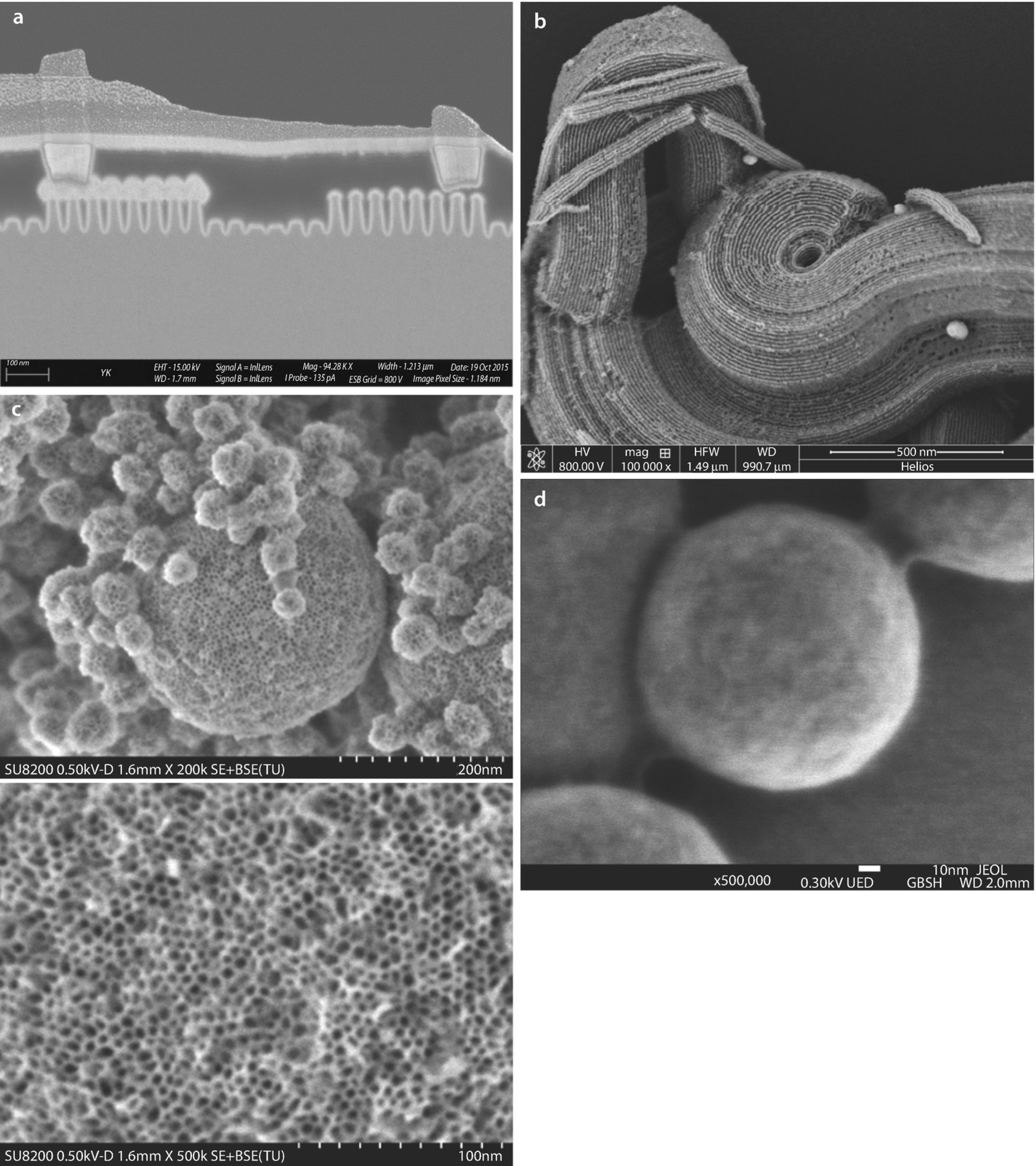
a High resolution SEM image taken at high beam energy ( E 0 = 15 keV) of a finFET transistor (16-nm technology) using an in-lens secondary electron detector. This cross section was prepared by inverted Ga FIB milling from backside (Zeiss Auriga Cross beam; image courtesy of John Notte, Carl Zeiss); Bar = 100 nm. b High resolution SEM image taken at low beam energy ( E 0 = 0.8 keV) of zeolite (uncoated) using a through-the-lens SE detector (image courtesy of Trevan Landin, FEI); Bar = 500 nm. c Mesoporous silica nanosphere showing 5-nm-diameter pores imaged with a landing energy of 0.5 keV (specimen courtesy of T. Yokoi, Tokyo Institute of Technology; images courtesy of A. Muto, Hitachi High Technologies); Upper image Bar = 200 nm, Lower image Bar = 100 nm. d Si nanoparticle imaged with a landing energy of 0.3 keV; Bar = 10 nm (image courtesy V. Robertson, JEOL)
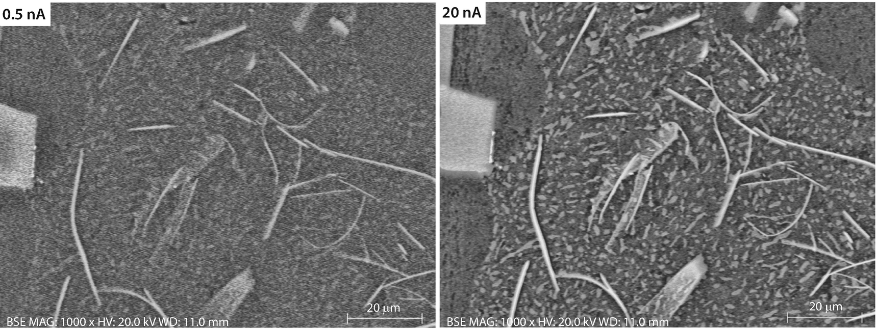
Effect of increasing beam current (at constant pixel dwell time) to improve visibility of low contrast features. Al-Si eutectic alloy; E 0 = 20 keV; semiconductor BSE detector (sum mode): ( left ) 0.5 nA; ( right ) 20 nA; Bar = 20 µm
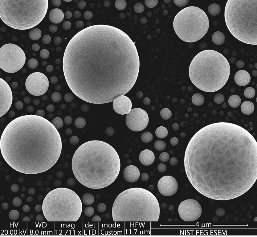
Large the depth-of-focus; Sn spheres; E 0 = 20 keV; Everhart–Thornley(positive bias) detector; Bar = 4 µm (Scott Wight, NIST)

Atomic number contrast with backscattered electrons. Raney nickel alloy, polished cross section; E 0 = 20 keV; semiconductor BSE (sum mode) detector. Note that four different phases corresponding to different compositions can be discerned; Bar = 10 µm
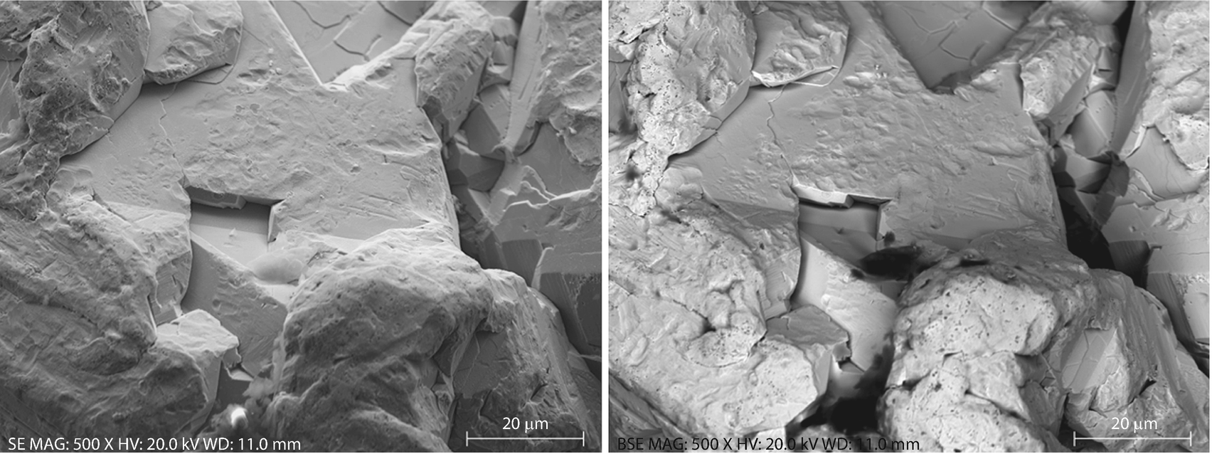
Topographic contrast as viewed with different detectors: Everhart–Thornley (positive bias) and semiconductor BSE (sum mode); silver crystals; E 0 = 20 keV; Bar = 20 µm
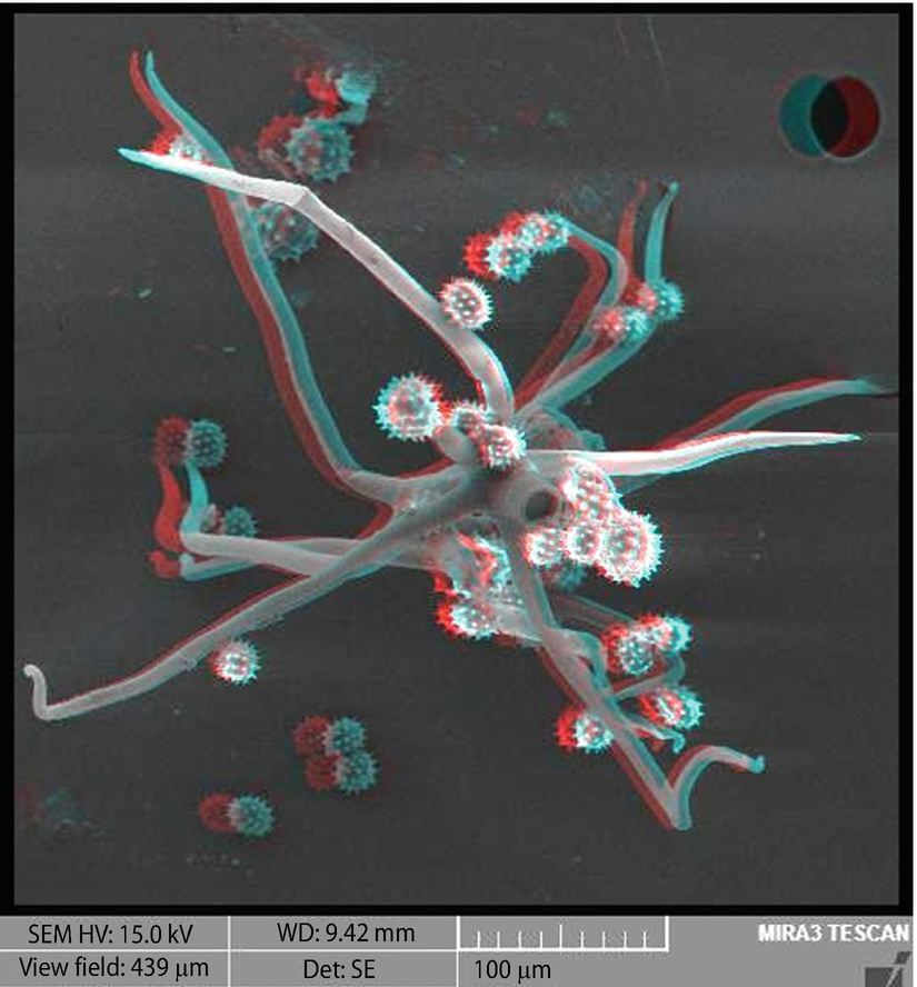
Visualizing the third dimension. Anaglyph stereo pair (red filter over left eye) of pollen grains on plant fibers; E 0 = 15 keV; coated with Au-Pd; Bar = 100 µm
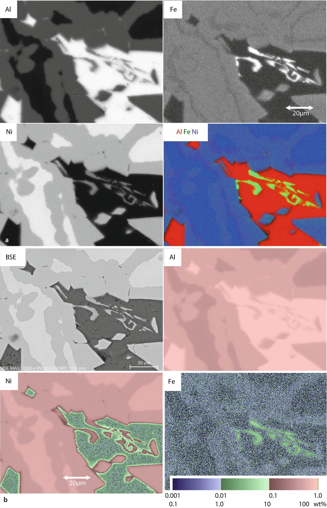
a EDS X-ray intensity maps for Al, Fe, and Ni and color overlay; Raney nickel alloy; E 0 = 20 keV. b SEM/BSE (sum) image and compositional maps corresponding to a
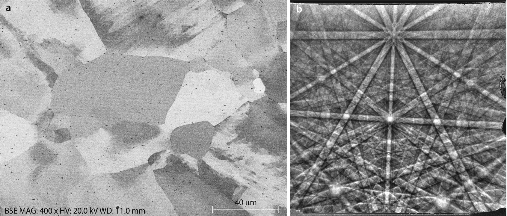
a Electron channeling contrast revealing grain boundaries in Ti-alloy (nominal composition: Ti-15Mo-3Nb-3Al-0.2Si); E 0 = 20 keV. b Electron backscatter diffraction (EBSD) pattern from hematite at E 0 = 40 keV
Measuring the Elemental Composition
“Major constituent”: 0.1 < C ≤ 1
“Minor constituent”: 0.01 ≤ C ≤ 0.1
“Trace constituent”: C < 0.01
The X-ray spectrum is measured with the semiconductor energy dispersive X-ray spectrometer (EDS), which can detect photons from a threshold of approximately 40 eV to E 0 (which can be as high as 30 keV). Vendor software supports collection and analysis of spectra, and these tools can be augmented significantly with the open source software National Institute of Standards and Technology DTSA II for quantitative spectral processing and simulation, discussed in this textbook.
Analytical software supports qualitative X-ray microanalysis which involves assigning the characteristic peaks recognized in the spectrum to specific elements. Qualitative analysis presents significant challenges because of mutual peak interferences that can occur between certain combinations of elements, for example, Ti and Ba; S, Mo, and Pb; and many others, especially when the peaks of major constituents interfere with the peaks of minor or trace constituents. Operator knowledge of the physical rules governing X-ray generation and detection is needed to perform a careful review of software-generated peak identifications, and this careful review must always be performed to achieve a robust measurement result.

![$$ \mathrm{RDEV}\left(\%\right)=\left[\left(\mathrm{Measured}-\mathrm{True}\right)/\mathrm{True}\right]\times 100\% $$](../images/271173_4_En_BookFrontmatter_OnlinePDF_TeX_Equ2.png)
An alternative “standardless analysis” protocol uses libraries of standard spectra (“remote standards”) measured on a different SEM platform with a similar EDS spectrometer, ideally over a wide range of beam energy and detector parameters (resolution). These library spectra are then adjusted to the local measurement conditions through comparison of one or more key spectra (e.g., locally measured spectra of particular elements such as Si and Ni). Interpolation/extrapolation is used to supply estimated spectral intensities for elements not present in or at a beam energy not represented in the library elemental suite. Testing of the standardless analysis method has shown that an RDEV range of ±25 % relative is needed to capture 95 % of all analyses.
High throughput (>100 kHz) EDS enables collection of X-ray intensity maps with gray scale representation of different concentration levels (e.g., ◘ Fig. 7a ). Compositional mapping by spectrum imaging (SI) collects a full EDS spectrum at each pixel of an x - y array, and after applying the quantitative analysis procedure at each pixel, images are created for each element where the gray (or color) level is assigned based on the measured concentration (e.g., ◘ Fig. 7b ).
Measuring the Crystal Structure
An electron beam incident on a crystal can undergo electron channeling in a shallow near-surface layer which increases the initial beam penetration for certain orientations of the beam relative to the crystal planes. The additional penetration results in a slight reduction in the electron backscattering coefficient, which creates weak crystallographic contrast (a few percent) in SEM images by which differences in local crystallographic orientation can be directly observed: grain boundaries, deformations bands, and so on (e.g., ◘ Fig. 8 ).
The backscattered electrons exiting the specimen are subject to crystallographic diffraction effects, producing small modulations in the intensities scattered to different angles that are superimposed on the overall angular distribution that an amorphous target would produce. The resulting “electron backscatter diffraction (EBSD)” pattern provides extensive information on the local orientation, as shown in ◘ Fig. 8b for a crystal of hematite. EBSD pattern angular separations provide measurements of the crystal plane spacing, while the overall EBSD pattern reveals symmetry elements. This crystallographic information combined with elemental analysis information obtained simultaneously from the same specimen region can be used to identify the crystal structure of an unknown.
Dual-Beam Platforms: Combined Electron and Ion Beams
Directionally-solidified Al-Cu eutectic alloy after ion beam milling in a dual-beam instrument, as imaged by the SEM column ( left image ); same region imaged in the HIM ( right image )
Modeling Electron and Ion Interactions
An important component of modern Scanning Electron Microscopy and X-ray Microanalysis is modeling the interaction of beam electrons and ions with the atoms of the specimen and its environment. Such modeling supports image interpretation, X-ray microanalysis of challenging specimens, electron crystallography methods, and many other issues. Software tools for this purpose, including Monte Carlo electron trajectory simulation, are discussed within the text. These tools are complemented by the extensive database of Electron-Solid Interactions (e.g., electron scattering and ionization cross sections, secondary electron and backscattered electron coefficients, etc.), developed by Prof. David Joy, can be found in chapter 3 on SpringerLink: http://link.springer.com/chapter/10.1007/978-1-4939-6676-9_3 .
References
Knoll M (1935) Static potential and secondary emission of bodies under electron radiation. Z Tech Physik 16:467
Knoll M, Theile R (1939) Scanning electron microscope for determining the topography of surfaces and thin layers. Z Physik 113:260
Oatley C (1972) The scanning electron microscope: part 1, the instrument. Cambridge University Press, Cambridge
von Ardenne M (1938) The scanning electron microscope. Theoretical fundamentals. Z Physik 109:553